
Linear SuperCap Charger with Current-Limited Ideal Diode and V/I Monitor

The LTC4425 provides a robust solution for charging applications requiring efficient energy management and precise voltage regulation. The dual-mode operation—LDO and normal mode—enhances versatility, allowing designers to adapt the charging strategy based on the application requirements. The smart charge current profile is particularly beneficial in preventing damage from inrush currents, thereby increasing system reliability.
The programmable output voltage feature allows for customization to specific application needs, while the active balancing circuit ensures longevity and performance of the supercapacitor stack by preventing overvoltage conditions. The choice of package dimensions facilitates integration into space-constrained designs, making the LTC4425 suitable for portable devices and compact electronic systems. Furthermore, the low quiescent current ensures minimal power draw during standby conditions, enhancing overall energy efficiency.
In summary, the LTC4425 is an advanced linear charger that combines low on-resistance, flexible charging modes, and intelligent current management, making it an excellent choice for applications involving supercapacitors and requiring precise voltage regulation.The LTC4425 is a constant-current/constant-voltage linear charger designed to charge a 2-cell supercap stack from either a Li-Ion/Polymer battery, a USB port, or a 2. 7V to 5. 5V current-limited supply. The part operates as an ideal diode with an extremely low 50m © on-resistance making it suitable for high peak-power/low average power applications.
The LTC4425 charges the output capacitors to an externally programmed output voltage in LDO mode at a constant charge current, or to VIN in normal mode with a smart charge current profile to limit the inrush current until the VIN to VOUT differential is less than 250mV. In addition the LTC4425 can be set to clamp the output voltage to 4. 9V or 5. 4V. Charge current (VOUT current limit) is programmed by connecting a resistor between PROG and GND. The voltage on the PROG pin represents the current fl owing from VIN to VOUT for current monitoring. An internal active balancing circuit maintains equal voltages across each supercapacitor and clamps the peak voltage across each cell to a pin-selectable maximum value.
The LTC4425 operates at a very low 20 A quiescent current (shutdown current <3 A) and is available in a low profile 12-pin 3mm G— 3mm DFN or a 12-lead MSOP package. 🔗 External reference
Related Circuits
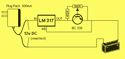
This circuit will charge a 12v battery (10 NiMH cells) @ approx 220mA. It is a very simple circuit but requires correct setting up. The circuit is designed around a 12vDC, 500mA plug pack. This type of plug pack...
In spite of the improvement of communication link and despite all progress in advanced communication technologies, there are still very few functioning commercial wireless monitoring systems, which are most off-line, and there are still a number of issues to...
There are many measurement systems that would be more suitable if a logarithmic scale is used, especially when attempting to mimic human sensory responses. Most... Logarithmic scales are particularly effective in representing a wide range of values in a compact...
The small DC voltages at the output of the diode detector are challenging to amplify accurately due to DC offsets introduced by any operational amplifier (op-amp) and low-frequency noise (1/f noise). A solution to these issues is to chop...
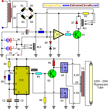
This document presents the circuit diagram of an IC-controlled emergency light with a charger, which functions as a 12V to 220V AC inverter circuit. The primary features of this circuit include automatic activation of the light during mains failure...

Utilizing sunlight as a power source can help reduce electricity costs. Below is a description of a simple power plant that can be created to charge a motorcycle battery or power emergency lights. Solar panels capture sunlight and convert...