
Logic Circuits Vs Transistor Power Circuits
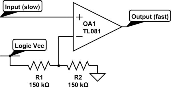
To achieve the goal of inverting a signal for driving FETs with fast rise and fall times, a discrete inverter circuit can be constructed using a combination of transistors. This design allows for greater control over the switching characteristics compared to standard logic chips. The key components in this circuit include a bipolar junction transistor (BJT) or a MOSFET configured as a NOT gate.
The basic operation involves using a resistor to pull the base of the BJT high when the 555 timer output is low, turning the transistor ON, which in turn pulls the output low. Conversely, when the 555 timer output is high, the transistor is turned OFF, allowing the output to rise. The choice of resistor values and the transistor type will significantly affect the rise and fall times of the output signal. It is essential to select a transistor with a suitable switching speed and ensure that the pull-up resistor is appropriately sized to achieve the desired performance.
When implementing this circuit, several considerations must be taken into account. The power supply voltage and current ratings of the FET being driven must be compatible with the output characteristics of the inverter circuit. Additionally, the layout of the circuit should minimize parasitic capacitance and inductance to ensure fast switching times. Proper decoupling capacitors should be placed near the power supply pins of the 555 timer and the inverter circuit to prevent voltage dips during switching.
Furthermore, it is crucial to understand the input and output impedance characteristics of the 555 timer and the inverter circuit. The output of the 555 timer should be capable of driving the base or gate of the inverter transistor without significant voltage drop. It may be beneficial to simulate the circuit using software tools to evaluate performance before physical implementation, ensuring that the desired switching characteristics are met.
In summary, building a discrete inverter circuit with careful attention to component selection and circuit layout will enable effective signal inversion for driving FETs. Understanding the nuances of logic circuitry and the specific requirements of the components involved will enhance the reliability and performance of the final application.Invert a signal to drive fets with hard/fast rise and fall times. I was told in another thread to use an inverter (NOT chip). This makes perfect sense to me since logic chips are always hard ON or OFF by design. But I`ve never worked with logic chips before. All I`ve dealt with is 555s and transistor/fet power circuits. Are there any `gotchas` or special things I need to know to implement a NOT chip into a 555 output to switch a FET without any hiccups For that matter, are there any `gotches` or things in general that apply to logic circuitry that someone with my background wouldn`t know and might stumble on 🔗 External reference
Related Circuits
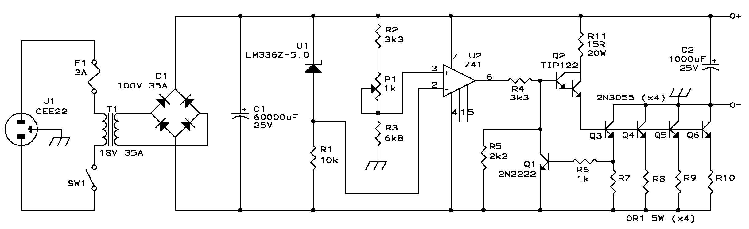
Build a 20 Amp 13.8 Volt Power Supply. There are some electronic applications where it may be necessary to run relatively high current circuits, such as transformers. To construct a 20 Amp, 13.8 Volt power supply, the following components and...
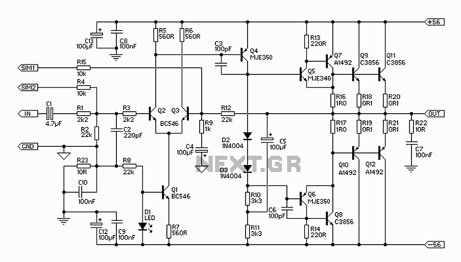
The 300W amplifier circuit presented is a conventional design. It includes connections for the internal SIM and incorporates filtering for RF protection (R1, C2). The input is facilitated through a 4.7µF bipolar capacitor, which offers substantial capacitance in a...
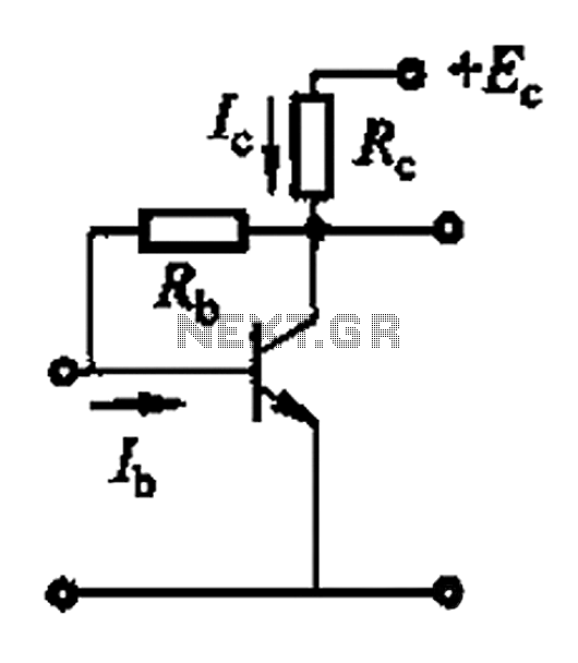
Basic reference bias circuit using a transistor with negative voltage feedback. The basic reference bias circuit utilizing a transistor with negative voltage feedback is designed to provide a stable output voltage or current that is largely independent of variations in...
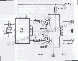
This converter features a central component, the CMOS 4047, which converts a 12V DC voltage into a 220V AC voltage. The 4047 operates as an astable multivibrator. At pins 10 and 11, a symmetrical rectangular signal is generated, which...
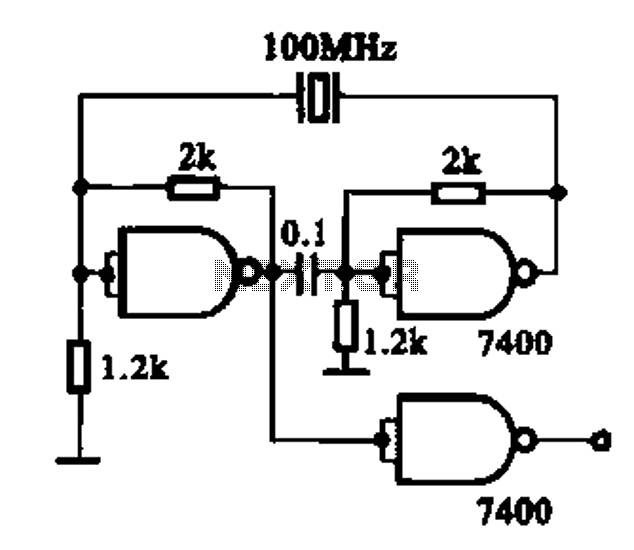
Crystal oscillator integrated circuits, specifically two diagrams of oscillator circuits with oscillation frequencies of 10 MHz and 20 MHz. Crystal oscillators are essential components in various electronic applications, providing stable frequency references for timing and synchronization purposes. The circuits presented...
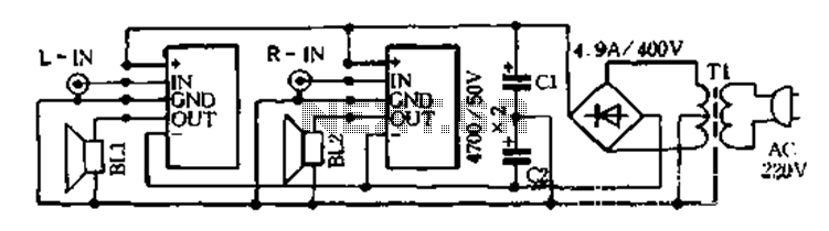
The D-200W module features a unique design that includes overload, overvoltage, overheating, short circuit, and reverse polarity protection, as well as shock protection for various speakers. The module employs a synchronous dynamic bias circuit to minimize static power consumption,...