
Loudspeaker Box Amplifier schematic
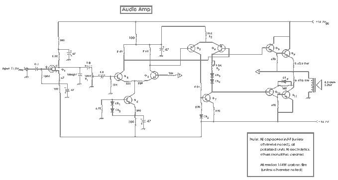
The selection of actual components is not critical. Any small signal "transistors anonymous" will work here. The only exception is Q8 and Q10. These two must be a 2N3904 and a 2N3906, as these are complimentary pairs. These transistors set the characteristics for the entire final, and must be balanced as to characteristics in order to keep DC out of the speakers, and for symmetrical amplification. As for the differential pairs (Q2, Q3, Q5, Q6) type isn't so important, however, matched pairs is important. It's a good idea to get a couple dozen of each, PNP and NPN, and select pairs that match closely in VBE and hFE. Matching pairs in the differential stages helps hold down DC offset, as this design uses DC coupling in the interest of good low frequency response. Speakers tend to object to any significant amount of DC by burning out the voice coils. It also compromises fidelity in that DC on the voice coils restricts the movement of the cone. The power supply is simply a straight forward symmetrical plus/minus supply constructed from a transformer with a balanced secondary and a bridge rectifier module. Even though the transformer was a self-wound unit, any transformer with a 25.2VCT secondary at 2.0A will be a good substitute. Such transformers ought to be available as VT "heater transformers" for high power "ham" RF amplifiers. It is essential that the primary side of the transformer be connected exactly as shown. This PS uses a MOV for over voltage protection. These things have a nasty habit of not turning off once they turn on. The fuse needs to be connected between this MOV and the mains. Don't attempt to "go cheap (or lazy)" and fail to include it. A 2.0A, "slow blow" type works well here. It will stand up to the initial surge as the filter capacitors charge up, and will prevent damage or worse should the MOV be triggered. This supply is somewhat over rated for the application, and is heavily bled for good voltage regulation. There is still some 120Hz hum that could be eliminated with a more involved PS circuit. However, as this wasn't intended as a "premium" amp, that wasn't necessary. The hum is most noticeable when running with no input signal. While actually playing sound, it's no longer noticeable. If you want to substitute a better supply, then that's OK, too. These units worked quite well, and do sound good, despite the inherent limitations of BJTs as analog amplifiers. There are a couple of improvements possible. The first would be the use of a full-complimentary final. If this is done, then any complimentary BJTs with a PC of 5.0W or more will work. Again, the most important part of this will remain the input Darlingtons. Even better would be the substitution of complimentary (N-Channel/P-Channel) VMOSFET power transistors. These, of course, don't require Darlington pairs in order to operate. If VMOS power transistors are used, it's important to include a 100-ohm resistor in series with the gate terminal, mounted close to the transistor body with the shortest lead length. This will help prevent the possibility of RF oscillation. (Unlike the BJT, the VFET is a high frequency device, and the inadvertent construction of VHF oscillators with these is quite easy.) The 1800pF capacitor connected to the drain of Q1 was included since one of these amps showed a weak (10mVP-P) oscillation at 700KHz. If you include it, be certain to make the connection with the least possible lead length, as it is an RF component. It will have no effect on the audio quality since its cutoff frequency is about 58KHz.
This design features a dual differential amplifier configuration, enhancing the linearity of the output transistors by introducing an additional feedback loop. The signal path consists of a series connection of the differential amplifier's inverting inputs, while feedback is provided to the non-inverting inputs, facilitating a more linear response. The absence of bypass capacitors in the constant current source ensures that the stage operates strictly in DC mode, which is critical for maintaining audio fidelity.
The output stage employs a semi-complementary configuration due to the limitations of component availability, specifically the lack of complementary pairs of BJTs at conventional retail outlets. This design choice is a compromise, as a fully complementary output stage would yield better fidelity. The maximum output is designed to be 6.0W, with a careful consideration of the speaker ratings to avoid damage from excessive power. The circuit's gain structure is set to limit output to safe levels while providing sufficient headroom for dynamic audio signals.
Transistor selection is crucial for maintaining performance, particularly for Q8 and Q10, which must be matched complementary pairs (2N3904 and 2N3906). The differential pairs should be closely matched in parameters to minimize DC offset and ensure symmetrical amplification. The power supply design is straightforward, utilizing a transformer with a balanced secondary and a bridge rectifier. The inclusion of a MOV for over-voltage protection and the necessity of a fuse are vital for safe operation.
Overall, the circuit is designed to deliver satisfactory audio performance while being constructed with readily available components. The potential for improvement exists, particularly through the use of fully complementary output stages or VMOSFET transistors, which would enhance the amplifier's capabilities and mitigate issues related to RF oscillation. The design also incorporates provisions for addressing oscillation concerns, ensuring stability in operation.This original design is a variation on a well-known design, examples of which can be found in a great many texts. My variation was to add a second differential stage to replace the usual common emitter-plus-constant current source.
Doing so opens up a second inverse feedback path. The signal path being a series connection of the differential amp inverting inputs, and the feedback being the non-inverting inputs. To this end, the constant current source does not include bypass capacitors to render it a DC-only stage.
The other feedback path is the usual one: output to the non-inverting input of the first differential stage. The idea is to add lots of inverse feedback in order to linearize the output transistors, as the non-linearity of these devices makes them rather poor analog amplifiers.
The other design criterion was the use of components readily available at a hobbist's store: "Radio Shack". No "exotic" components that would require a special order are used here. To this end, the output stage is a semi-complementary design, although this is not optimum so far as fidelity is concerned.
(Radio Shack doesn't offer complimentary pairs of power BJTs.) Since the amp is intended to work into the "wide band" (60Hz -- 18KHz) speakers that this store sells, the gain is deliberately kept down. With the design given here, the max output is 6.0W. Even here, since these speakers are rated at 3.0W, you could blow speakers if the volume is turned up too high.
Limiting output is accomplished with the initial voltage amp (Q1). This stage has a gain of 7.5, so that with a 1.0VRMS input, the output voltage becomes slightly less than 7.5VRMS. The gain of the circuit from the output end of the volume control to the speaker is unity, due to the large negative feedback.
You could drive the power output as high as 10W, as there is plenty of "head room" in the power supply design. (Again, this was done to improve the fidelity as much as possible with a BJT-based design.) If you push the output, you will need better heat sinking on the finals than what's described here.
The selection of actual components is not critical. Any small signal "transistors anonymous" will work here. The only exception is Q8 and Q10. These two must be a 2N3904 and a 2N3906, as these are complimentary pairs. These transistors set the characteristics for the entire final, and must be balanced as to characteristics in order to keep DC out of the speakers, and for symmetrical amplification. As for the differential pairs (Q2, Q3, Q5, Q6) type isn't so important, however, matched pairs is important.
It's a good idea to get a couple dozen of each, PNP and NPN, and select pairs that match closely in VBE and hFE. Matching pairs in the differential stages helps hold down DC offset, as this design uses DC coupling in the interest of good low frequency response.
Speakers tend to object to any significant amount of DC by burning out the voice coils. It also compromises fidelity in that DC on the voice coils restricts the movement of the cone. The power supply is simply a straight forward symmetrical plus/minus supply constructed from a transformer with a balanced secondary and a bridge rectifier module. Even though the transformer was a self-wound unit, any transformer with a 25.2VCT secondary at 2.0A will be a good substitute.
Such transformers oughht to be available as VT "heater transformers" for high power "ham" RF amplifiers. It is essential that the primary side of the transformer be connected exactly as shown. This PS uses a MOV for over voltage protection. These things have a nasty habit of not turning off once they turn on. The fuse needs to be connected between this MOV and the mains. Don't attempt to "go cheap (or lazy)" and fail to include it. A 2.0A, "slow blow" type works well here. It will stand up to the initial surge as the filter capacitors charge up, and will prevent damage or worse should the MOV be triggered.
This supply is somewhat over rated for the application, and is heavily bled for good voltage regulation. There is still some 120Hz hum that could be eliminated with a more involved PS circuit. However, as this wasn't intended as a "premium" amp, that wasn't necessary. The hum is most noticeable when running with no input signal. While actually playing sound, it's no longer noticeable. If you want to substitute a better supply, then that's OK, too. These units worked quite well, and do sound good, despite the inherent limitations of BJTs as analog amplifiers.
There are a couple of improvements possible. The first would be the use of a full-complimentary final. If this is done, then any complimentary BJTs with a PC of 5.0W or more will work. Again, the most important part of this will remain the input Darlingtons. Even better would be the substitution of complimentary (N-Channel/P-Channel) VMOSFET power transistors. These, of course, don't require Darlington pairs in order to operate. If VMOS power transistors are used, it's important to include a 100 ohm resistor in series with the gate terminal, mounted close to the transistor body with the shortest lead length.
This will help prevent the possibility of RF oscillation. (Unlike the BJT, the VFET is a high frequency device, and the inadvertant construction of VHF oscillators with these is quite easy.) The 1800pF capacitor connected to the drain of Q1 was included since one of these amps showed a weak (10mVP-P) oscillation at 700KHz. If you include it, be certain to make the connection with the least possible lead length, as it is an RF component.
It will have no effect on the audio quality since its cutoff frequency is about 58KHz. 🔗 External reference
Related Circuits
This page contains some information on circuits which can be used for triggering stroboscopes from external circuits. The circuits here are designed to be integrated into stroboscope circuits so that they can be triggered using an external trigger pulse....
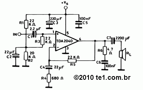
The TDA2040 is a monolithic integrated circuit housed in a Pentawatt package, designed for use as an audio class AB amplifier. It typically delivers an output power of 22W (with a distortion factor of 0.5%) at a supply voltage...
A current meter is employed to measure the current generated by a solar panel, exhibiting minimal power loss for currents within the 0-10A range. It also serves as a general-purpose DC current meter. The Gate Boost Solar Engine utilizes...
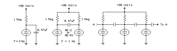
In this circuit, one, two or three neon indicator bulbs can be made to flash in sequence at rates determined by the R and C values. In the single stage circuit, using one lamp, the capacitor charges through the...
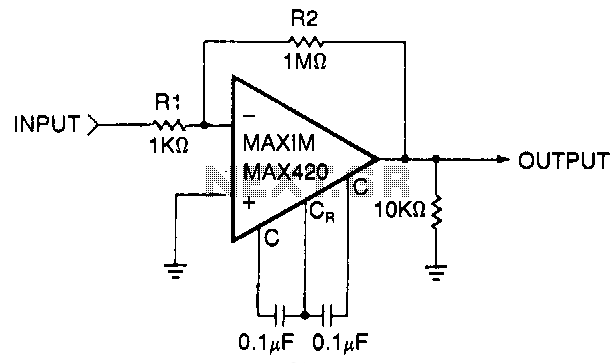
This circuit is a gain-of-1000 inverting amplifier designed to amplify submillivolt signals to levels suitable for further processing. In most system applications, utilizing maximum gain in the MAX420 is advantageous, as it minimizes the effects of offsets in later...
Design a lighting circuit for an indoor garden. There is a 24V input source that needs to be limited to 20V. LA is a series array of LEDs with a total voltage drop of approximately 19.8V. R1 and Z1...