
low noise oscillator design

The first step in improving oscillator performance is enhancing the power supply. Typically, circuits within the amateur radio community utilize some form of linear voltage regulator to stabilize the supply voltage to a fixed level. However, linear voltage regulators tend to introduce a considerable amount of noise into the system. A high noise floor in the supply voltage directly impacts the output signal of the oscillator, as the noise modulates the oscillator circuit, resulting in increased phase noise. Fortunately, a simple solution exists: a low-pass filter. Implementing a basic RC low-pass filter, composed of R1 and C3, on the output of the linear voltage regulator significantly reduces supply voltage noise. Additionally, C4 serves as a block capacitor, designed to eliminate short spikes in the supply voltage. This minor addition is cost-effective and can be easily implemented by anyone. Consistently incorporating a low-pass filter after a linear voltage regulator will lead to substantial improvements in the overall noise figure of the circuit. Furthermore, a block capacitor in the supply voltage path before any critical components, such as integrated circuits (ICs) or transistors, is also highly recommended.
The second enhancement involves the RF output. Instead of deriving the RF output from the collector of T1, the circuit employs a capacitive voltage divider, comprising C5 and C6. Ideally, the reactance of C5 should be minimized in relation to C6. As any capacitive or inductive load on the output can slightly detune the crystal's frequency, the inclusion of a buffer amplifier is essential before routing the RF signal to any other circuitry. It is also advisable to incorporate an additional low-pass filter on the output of the RF buffer amplifier to effectively suppress harmonics of the RF signal.
In summary, these improvements focus on enhancing the stability and purity of the oscillator's output, thereby ensuring better overall performance in RF applications.The overall performance of any rf circuit in regards of it`s phase noise and spectral purity depends significantly on the frequency generating circuitry, commonly an oscillator. Low noise oscillators with high spectral purity are neither witchcraft nor black magic. Many people think the design of oscillators is black magic as such circuits usually either work or not. Especially beginners are glad when they finally get a circuit to oscillate and attributes such as signal quality are usually secondary and often neglected. This article is going to show two easy tricks that can be implemented in almost any oscillator design.
To be precise, the oscillator is a Miller crystal oscillator. In case you are wondering where the LC tank circuit in the collector path of T1 is, look closer! The inductor L1 has an unavoidable capacitance known as parasitic capacitance` or stray capacitance`. I personally prefer the term parasitic capacitance because the term stresses that the capacitance is a (usually) unwanted phenomena.
Parasitic capacitance is the reason why inductors have a self-resonance frequency (SRF) mentioned in their datasheet. The first step is to improve the power supply. Usually circuits in the amateur radio community use some sort of linear voltage regulator to stabilize the supply voltage to a fixed voltage.
Linear voltage regulators have the unfortunate habit of introducing a significant amount of noise into the system. [ 1 ] It should be apparent that a high noise floor in the supply voltage has a direct influence on the output signal of an oscillator.
The noise directly modulates the oscillator circuit and produces plenty of phase noise. Luckily, there`s an easy remedy for this problem; a low pass filter. A simple RC low pass filter, consisting of R1 and C3, on the output of the linear voltage regulator improves the supply voltage noise drastically. C4 is a block capacitor and is supposed to short out all kinds of short spikes in the supply voltage.
Just this tiny add-on is cheap and can be implemented by anyone. If you discipline yourself to always include a low pass filter after a linear voltage regulator you will see great improvement in the overall noise figure of your circuit. A block capacitor in the supply voltage path in front of any significant part of a circuit, such as an ICs or transistors, should be considered mandatory also.
The second improvement I implemented is the rf output. Instead of taking the rf output from the collector of T1, the circuit uses a capacitive voltage divider, consisting of C5 and C6. Ideally, the reactance of C5 is chosen as small as possible in regards to C6. Since any capacitive or inductive load on the output will slightly detune the crystals frequency, a buffer amplifier is absolutely necessary before applying the rf to any other circuitry.
It goes without saying that there should be another low pass filter on the output of the rf buffer amplifier to suppress harmonics of the rf signal effectively. [1] Analog Applications Journal (2005): John C. Teel. Understanding noise in linear regulators. Texas Instruments Incorporated. 🔗 External reference
Related Circuits
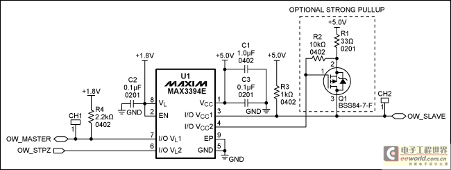
The designer requires a 1-Wire host computer IO framework that operates at 1.8V. Most 1-Wire devices are unable to function at this voltage. This application recommends implementing a 1.8V 1-Wire host computer alongside a 5V 1-Wire reference design for...

This is a design circuit for a Colpitts crystal oscillator. It is suitable for low-frequency crystal oscillator applications. Utilizing the 2N3823 JFET, this circuit exhibits excellent stability as temperature variations do not affect the loading of the 2N3823 JFET...
In a basic astable timer configuration, timing periods 11 and 12 are not independently controlled. This lack of control complicates the maintenance of a constant period, T, when either 11 or 12 is varied. In this circuit, the charge...

The robot was controlled using a Motorola 68HC11 on a special MC11 input/output board provided by the Stanford Smart Product Design Lab (SPDL). The SPDL also supplied motor controller boards, each consisting of a DS3658 stepper controller, an SN754410...
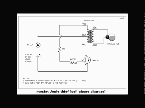
Joule thief circuit using MOSFET. The Joule Thief is a minimalist circuit designed to extract energy from low-voltage sources, such as depleted batteries, by utilizing a self-oscillating boost converter topology. This circuit is particularly useful for powering small electronic devices...
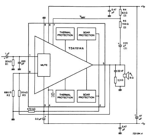
The TDA1514 audio amplifier circuit design is an electronic project capable of delivering high audio power output using a specialized audio integrated circuit (IC) and a few common components. Manufactured by Philips Semiconductor, the TDA1514 audio IC can provide...