
Low Power Voltage Reference
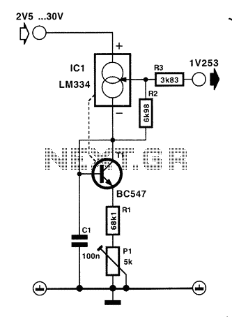
The LM334 current source is a versatile component widely used in precision voltage reference applications due to its ability to provide a stable output current with minimal temperature drift. In the described circuit, the LM334 is configured to deliver a constant current, which is critical for maintaining the stability of the output voltage across varying temperatures and input conditions. The choice of a low-temperature coefficient is essential in applications where precision is paramount, such as in analog-to-digital converters or voltage reference circuits.
The implementation involves careful selection of resistors, particularly R1, which is used to set the output voltage. The recommendation to use metal film resistors ensures low noise and high stability, which are crucial for maintaining the integrity of the output voltage. The use of a potentiometer (P1) allows for initial tuning of the output voltage, after which it should be replaced with a fixed resistor to avoid any future adjustments that could introduce variability.
The negative resistance of 3.8 kΩ at the output is an important characteristic, as it contributes to the overall stability of the circuit by compensating for any potential variations in load conditions. The output impedance of 400 Ω is also a critical parameter, as it influences how the circuit interacts with the load, ensuring that the voltage remains stable even under varying load conditions.
The circuit's performance under different input voltages demonstrates its robustness, with only a minimal change in output voltage noted across a wide input range. This feature is particularly beneficial in applications where the power supply voltage may fluctuate. The low thermal coefficient, ideally reduced to 5 ppm/°C with careful adjustments, highlights the circuit's capability to maintain a consistent reference voltage over a range of environmental conditions, making it suitable for precision instrumentation and other sensitive electronic applications.The voltage reference circuit described below, is a special implementation of current source LM334. Characterized by a very small temperature coefficient metatholio output voltage and consumes only 10uA room temperature. This current fluctuates by a few uA, when the ambient temperature varies significantly. The positive rate of temperature change LM334 offset by the negative of the contact base emitter transistors has a direct thermal coupling with the integrated.
To achieve the lowest possible temperature coefficient, it is necessary to adjust the output voltage of 1,253 V source to the arrangement easily done through R1.
From the moment you get the desired output voltage, you are advised to stuck P1 and after the count value, replace it with a constant resistance. The best indeed is to replace P1 with the R1, so you have fewer parts. Prefer metal film resistors and tolerance of 1% E96 series. Having as a given that the output voltage obtained from the pin configuration LM334, is expected to show a negative resistance value 3.8 KO.
The resistance A3 ensures that the output impedance will be equal to 400 W. Under these conditions, the current that can provide the source to the load to be connected to out of retained less than 5 Ma stability of the voltage source is more than satisfactory. By varying the input voltage from 5 V to 30 V, the change in output was only 0.6 mem (from 1.2530 to 1,2536 V).
The change in the thermal coefficient is maintained at values ??less than 50 ppm / C, and if you worry a bit more to the setting of the circuit, you will see that quite easily reaches 5 ppm / C. The requirements of the original circuit current was only 9.8 mA at a temperature of 22C.
Related Circuits
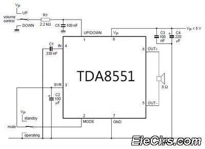
An amplifier with digital volume control can be designed predictably due to the simplicity of the circuit, which utilizes a single chip, the TDA8551. This series of mini amplifiers with digital volume control operates as a BTL (Bridge-Tied Load)...
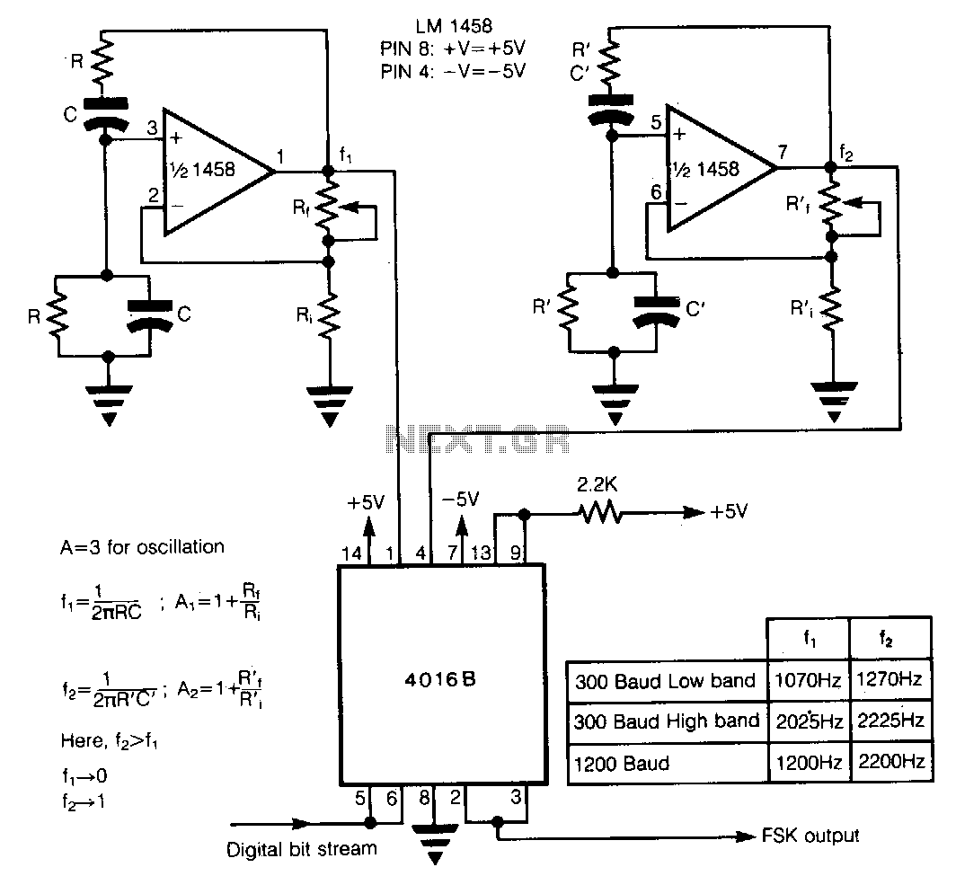
In Frequency Shift Keying (FSK), two distinct frequencies are utilized to represent the binary digits 0 and 1. The core of the circuit comprises two Wien-bridge oscillators constructed with a dual operational amplifier LM1458, each generating one of the...
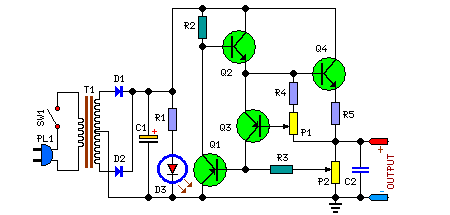
The transformer can be selected based on the required maximum voltage and current output. Recommended options include: 36V, 40V, or 48V center-tapped configurations, with power ratings of 50VA, 75VA, 80VA, or 100VA. It is essential to mount Q4 on...
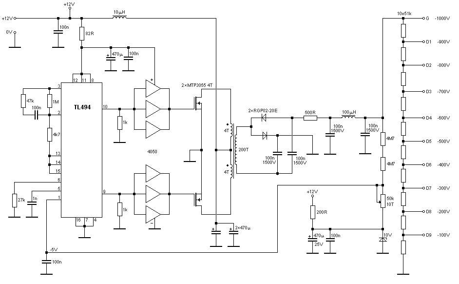
The schematic diagram originates from a circuit designed for a stable power supply ranging from -100V to -1000V. For further details, refer to the page that explains the circuit diagram associated with this power supply. This stable power supply...
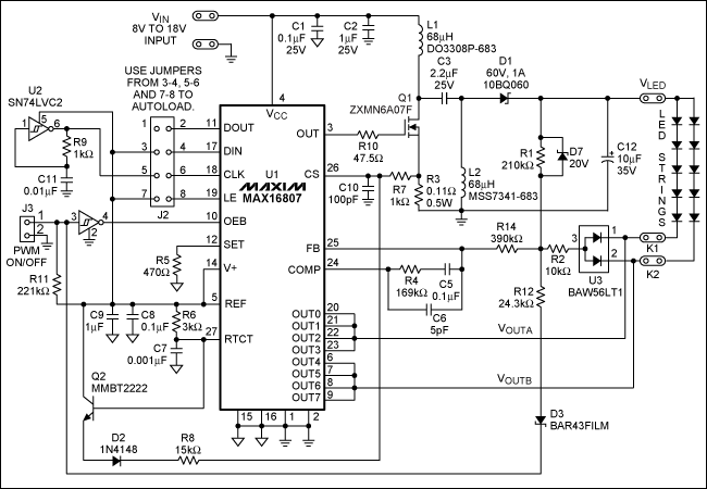
This application note discusses the use of SEPIC power modules to supply the necessary power for driving high-brightness LED arrays. These arrays serve as display backlights and necessitate a wide dimming range. The SEPIC configuration offers an efficient and...
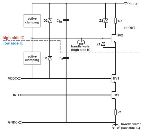
Integration of 1200V SOI gate driver ICs into a medium power IGBT module package. A novel approach for medium power applications. The integration of 1200V Silicon-On-Insulator (SOI) gate driver Integrated Circuits (ICs) into medium power Insulated Gate Bipolar Transistor (IGBT)...