
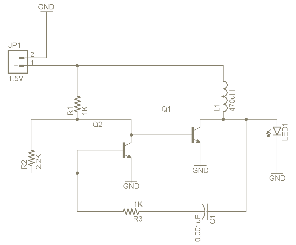
make this simple delay on circuit

An automatic voltage stabilizer rated at 1KVA exhibits a defect where it outputs a very high voltage for approximately 1.5 seconds upon activation, causing frequent failure of CFLs and bulbs. After this initial period, the voltage stabilizes to acceptable levels. The internal structure of the stabilizer includes an auto-transformer and four 24V relays, each linked to a separate circuit. Each circuit consists of a 10K preset resistor, a BC547 transistor, a zener diode, a BDX53BFP NPN Darlington pair transistor IC, a 220µF/63V capacitor, a 100µF/40V capacitor, four diodes, and various resistors. These circuits are powered by a step-down transformer, with outputs taken across the respective 100µF/40V capacitors and directed to the corresponding relays.
To address the issue, potential fault sources include a relay momentarily switching ON and connecting incorrect contacts to the output or a relay taking a brief period to stabilize at the correct voltage after power activation. Given the presence of multiple relays, diagnosing and rectifying the fault may be complex. Implementing the delay ON timer circuit described could effectively resolve the issue by ensuring that the output is activated after a delay, allowing the internal relays sufficient time to stabilize at the correct voltage levels across their output contacts.
This delay ON circuit can be constructed using a 12V DC power supply, a resistor (R2), a capacitor (C2), and two transistors (T1 and T2) configured as a switching mechanism. The capacitor (C2) charges through the resistor (R2) when power is applied, and the time constant of this RC circuit determines the delay duration. The zener diode can be included to provide a stable reference voltage for the base of T1, ensuring consistent operation regardless of minor fluctuations in the power supply. The output relay can be selected based on the load requirements, and proper heat dissipation measures should be taken for the transistors to prevent thermal runaway during operation.
In summary, the integration of a delay ON circuit into the existing voltage stabilizer design can mitigate issues related to premature voltage spikes by ensuring that the output is only activated after the internal components have stabilized, thereby enhancing the reliability and longevity of connected devices.The post explains a simple delay ON circuit which allows the connected load at the output to be switched ON with some predetermined delay after power switch ON. The explained circuit can be used for all applications which calls for an initial delay ON feature for the connected load after the mains power is switched ON.
The shown diagram is pre tty straightforward yet provides the necessary actions very impressively, moreover the delay period is variable making the set up extremely useful for the proposed applications. Assuming the load which requires the delay ON action being connected across the relay contacts, when power is switched ON, the 12V DC passes via R2 but is unable to reach the base of T1 because initially, C2 acts as a short across ground.
Once C2 charges up to a level which develops a potential of 0. 3 to 0. 6V (+zener voltage) at the base of T1, T1 is instantly switched ON, toggling T2, and the relaysubsequently. finally the load gets switched ON too. I have a 1KVA automatic voltage stabilizer. It has one defect that when it is switched on, very high voltage is outputted for about 1. 5s (therefore cfls and bulb got fused frequently) after that the voltage becomes OK. I have opened the stabilizer it consist of an auto-transformer, 4 24V relay each relay connected to aseparatecircuit(each consisting of 10K preset, BC547, zener diode, BDX53BFP npn darlington pair transistor IC, 220uF/63v capacitor, 100uF/40V capacitor, 4 diodes and some resistors).
These circuits are powered by a step down transformer and output of these circuit are taken across corresponding 100uF/40V capacitor and fed to corresponding relay. What to do in order to tackle the problem. please help me. Hand drawn circuit diagram is attached. The problem in the above circuit might be due to two reasons: one of the relays is switching ON momentarily connecting the wrong contacts with the output, or one of the responsible relays is settling down with the correct voltages a little while after power switch ON.
Since there are more than one relay, tracing out the fault and correcting it can be a bit tedious. the circuit of a delay ON timer explained in the above article could be actually very effective for the discussed purpose. The above wiring would instantly take care of the issues as now the output would switch after some time during power witch ONs, allowing enough time for the internal relays to settle down with the correct voltages across their output contacts.
🔗 External reference
Related Circuits
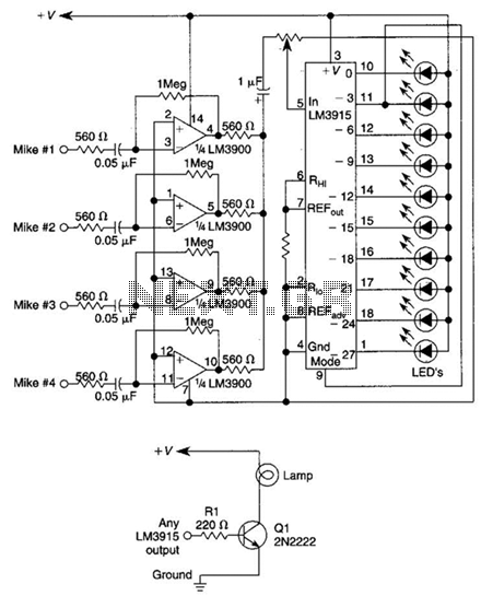
This circuit will produce an output when the sound exceeds a preset level. The LM3915 is a log-output bar graph driver. A transistor driver is used for higher current loads. To drive heavy-current loads with an LM3915 output, a...

A series of LEDs that turn on and off in a precise sequence, creating a calming and hypnotic effect. Various LED chaser, scanner, and sequencer circuits exist, utilizing discrete transistors, logic integrated circuits (ICs), or microcontrollers. However, a common...
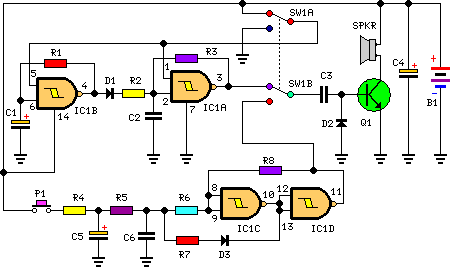
This circuit is designed for children's entertainment and can be installed on bicycles, battery-powered cars, motorcycles, as well as on models and various games and toys. When switch SW1 is positioned as depicted in the circuit diagram, it generates...
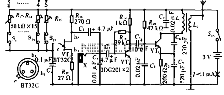
The circuit operates with VT3 and associated components arranged as a common-base capacitance feedback oscillation circuit. The oscillation frequency is set by capacitors C8, C9, and inductor L1. VT2 serves as a voltage amplification stage that reinjects the audio...
Samsung C3330 Circuit Diagram Download Manual PDF Download. The Samsung C3330 circuit diagram serves as a comprehensive reference for understanding the electronic architecture of the device. This schematic provides detailed insights into the interconnections between various components, including the microcontroller,...
The Joule Thief is a straightforward and uncomplicated device, yet its functionality is remarkable. It can utilize a battery that is otherwise deemed unusable in any other electronic device, and it is very easy to construct on a breadboard...