
Making a 900MHz Phone Bug
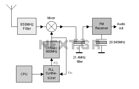
The project involves the utilization of a 900MHz cordless phone, specifically designed to operate within the 914MHz to 959MHz frequency range. The circuit architecture can be divided into distinct functional blocks, primarily the transmitter and receiver sections. The transmitter section, which operates at 914MHz, includes a filter and preamplifier, while the receiver section is designed to receive signals at 959MHz.
The RF signal is processed through a series of stages beginning with filtering and amplification at 959MHz. This signal is subsequently fed into a mixer, where it is down-converted to a lower frequency for further processing. The mixer receives its input from a Voltage Controlled Oscillator (VCO), which is critical for generating the necessary frequency. The VCO is controlled by a Phase-Locked Loop (PLL) synthesizer, which continuously monitors the VCO frequency and adjusts the control voltage to maintain a stable output frequency.
The PLL synthesizer features a phase detector (PD) output that modulates the varicap diode within the VCO circuit, enabling fine-tuning of the oscillation frequency. The VCO output signal is typically weak; thus, it is amplified by a transistor (Q2) before being routed to the mixer. Additionally, a portion of the VCO output is tapped off and amplified by another transistor (Q3) to provide feedback to the PLL for frequency monitoring.
The system incorporates a ceramic filter designed for 455kHz, which is utilized in the FM demodulation process. This filter is integral to the receiver circuit, ensuring that only the desired frequency components are passed through for demodulation. The overall design emphasizes the importance of precise frequency control and signal integrity, which are essential for effective communication in cordless phone applications.
The schematic representation of this circuit would typically include symbols for the various components such as the VCO, PLL, mixers, filters, and transistors, along with appropriate connections indicating the flow of signals throughout the system. This comprehensive understanding of the circuit components and their functions is crucial for anyone looking to replicate or modify similar cordless phone systems.Today they have moved up to 900MHz. It is not easy to build stuff for 900MHz so in this project I will re-use an old cordless 900MHz phone I found in a container. Since you wont have the same phone as I have, you might think this is not a project for you, Wrong! Read this and you will learn how do identify parts in cordless phones and you can rebuild almost any model.
This is a block diagram of an analogue 900MHz cordless phone. The transmitter part is not interesting because we don't want to transmit anything. The RF signal is first filtered and amplified in a 959 MHz filter. The RF signal will then enter a mixer to be down converted to lower frequency. To the mixer you will find a VCO (Voltage Controlled Oscillator). The frequency from the VCO is controlled by a PLL synthesizer. The PLL synthesizer probes the VCO frequency (Fin), and adjust the "PD" voltage until it finds and locks to the programmed frequency. The product out of the mixer will pass a filter (21.4MHz in my case) and then enter a standard FM receiver circuit to demodulate the sound.
In my phone I found a shielded box of 4x4 cm. I removed the cover and took some photos. To left you can see the antenna as a spiral. There is four section in my box. The first thing we see is a black circuit in the blue frame, three yellow boxes in the green and red frame and outside the box you will see a crystal and a black box with text "455D" and under that some kind of tuneable coil. I know that the cordless phones receive at 959MHz and transmit at 914MHz. If you look again in the red and green frames you will find two yellow cubes with label 959 and in the red frame 914.
This yellow cube things is filters and preamplifier. Now we can easy understand that the red frame is the transmitter part and the green is the receiver part. The blue frame has an ic circuit. It is the PLL synthesizercircuit. Finally the yellow frame is the VCO. You may think it is not this easy to identify all block, but I will now look into each frame and I will show you details that will confirm the function of each block.
The picture above show you the yellow frame, the VCO. I have removed the PLL circuit because we don't need it and it hides the wires on the pcb. A VCO is an oscillator which is voltage controlled. The oscillating components are a coil and a capacitor. To change the frequency you need the capacitance to be voltage controlled. This is done by a varicap. In the PIC above you will find the varicap and the coil at the bottom. The LC circuit needs a transistor to keep it oscillating and this transistor is Q1. If you follow the strip line of the pcb you can actually see that the coil and varicap is connected to this transistor. In my block diagram you can see that the PLL circuit has an output called PD which is connected to the varicap to set the VCO voltage.
If you follow the strip line of the varicap to the right and through two resistors you end up at the PLL circuit. The VCO signal from Q1 is not so strong and is amplified in Q2 and goes out of the yellow frame through a hole (Fout) to the mixer (I show you later).
So what does Q3 do? Look again at the block diagram and you will find that the PLL need to probe the VCO to know the frequency of the VCO. A small portion of the VCO signal is amplified by Q3 and then goes to the PLL (Fin). Outside the shielded case you will se a crystal and under the crystal (you can not se it on this pic) is a 16 pin SO IC-circuit MC3371.
If I look into the datasheets I find that this circuit is a FM receiver. The black box below the crystal with the label 455 is easy to identify, it is a ceramic filter for 455kHz. Below that box is a tuneable coil which must be the quad coil. 🔗 External reference
Related Circuits
The microphone issue on the Nokia 6630 is typically attributed to several factors, including a damaged microphone, a broken circuit path, or a faulty UEM IC. If the issue arises from a broken path in the microphone circuit, it...
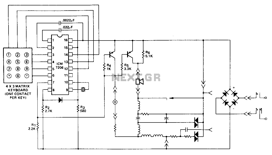
This encoder utilizes a single contact per key keyboard and implements all other switching functions electronically. A diode is positioned between terminals 8 and 15 to prevent the output from exceeding 1 volt negative in relation to the negative...
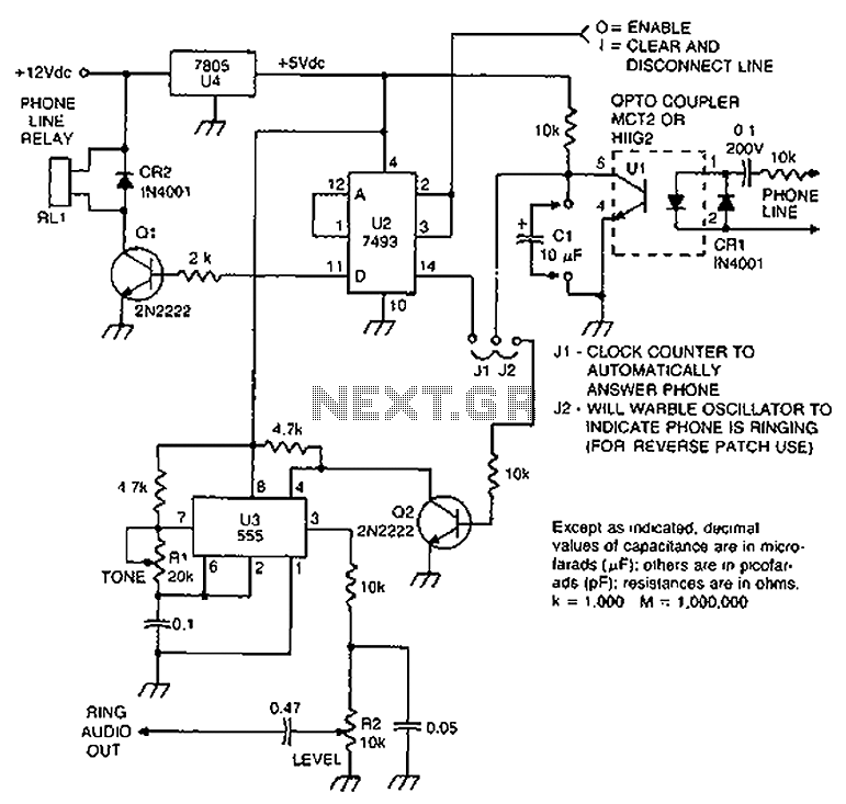
Check the loop circuit for an automatic telephone answering system or a tone generator for use in reverse automatic repair. The loop circuit in an automatic telephone answering system is designed to detect incoming calls and activate the answering mechanism....

Utilize standard RF wiring precautions. Optimal speech clarity is achieved by employing an electret microphone. For music reproduction, replace it with a dynamic microphone element. In the design of audio circuits, particularly those involving speech and music, the choice of...

This add-on device for telephones can be connected in parallel to the telephone instrument. The circuit provides audio-visual indication of on-hook, off-hook, and ringing modes. It can also be used to connect the telephone to a CID (caller identification...

The Telephone Totalizer is built around two 4518 dual synchronous up counters, a 74C925 4-digit counter, a 458 hex inverting buffer, and a 4081 quad 2-input AND gate. It is designed to estimate toll charges by calculating the time...