
Micropower double ended limit detector
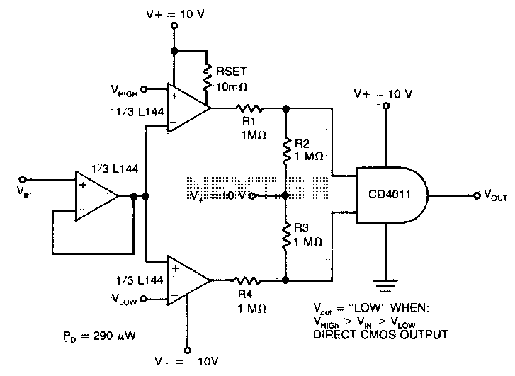
The circuit employs four 1 megohm resistors, R1, R2, R3, and R4, which serve to convert the bipolar ±10V swing of the operational amplifiers to a 0 to 5V swing that is compatible with ground-referenced CMOS logic.
The primary function of this voltage monitor is to provide a reliable indication of whether the input voltage is within the predefined thresholds. The L144 sections act as voltage comparators, monitoring the input voltage against the set limits, Vhigh and Vlow. When Vin exceeds Vhigh, or falls below Vlow, the output of the NAND gate transitions to a logical high state, signaling that the monitored voltage is outside the acceptable range. Conversely, when Vin is within the specified limits, the output remains low.
The choice of using a CMOS NAND gate is significant due to its low power consumption characteristics, making it suitable for battery-operated devices or applications where power efficiency is critical. The resistors R1 through R4 play a crucial role in ensuring that the analog signals from the operational amplifiers are scaled down appropriately to avoid damage to the CMOS logic and to ensure accurate logical interpretation.
In summary, this voltage monitor circuit effectively combines the functionality of operational amplifiers and CMOS logic to provide a robust solution for monitoring voltage levels in various electronic applications, ensuring that the output accurately reflects the input voltage conditions.The detector uses three sections of an L144 and a DC4011 type CMOS NAND gate to make a very low power voltage monitor. If the input voltage, Vin, is above Vhigh or below Vlow, the output will be a logical high. If (and only if) the input is between the limits will the output be low
The 1 megohm resistors Rl, R2, R3, and R4 translate the bipolar ±10V swing of the op amps to a 0 to LOV swing acceptable to the ground-referenced CMOS logic.
🔗 External referenceRelated Circuits
Men often appreciate the convenience of television remote controls, which can sometimes frustrate their female partners. They tend to switch channels frequently, wanting to ensure they do not miss anything while a specific program is on. With the remote...
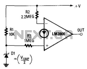
The output becomes high when the supply voltage drops below a threshold set by the zener diode D1. If D1 is a 5.6-V zener diode, the operational amplifier will activate when the supply voltage decreases to around 11 V....
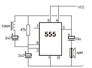
This metal detector electronic project schematic circuit is designed using a simple 555 timer integrated circuit. The schematic circuit requires a few external electronic components. The metal detector circuit utilizes the 555 timer IC in astable mode to generate a...

Once again, this is a project designed by David Sayles. The input can be from a longwire or a loop antenna. The unit covers MW and Sw to 30MHz. This project involves a versatile antenna interface designed to accommodate...
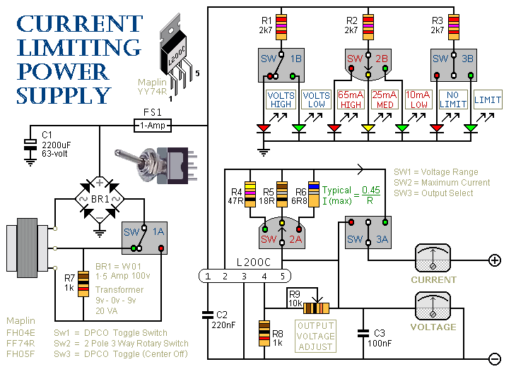
This is a 1-amp variable-voltage PSU. It adjusts from about 3v to 24v and has the added feature that you can limit the maximum output current. This is invaluable when, for example, you power-up a project for the first...
The PTB78560x is a series of 30 W rated isolated DC/DC converters designed to operate from a standard 24 V or 48 V telecom central office (CO) supply. Housed in a 12 package, each model features a wide adjustable...