
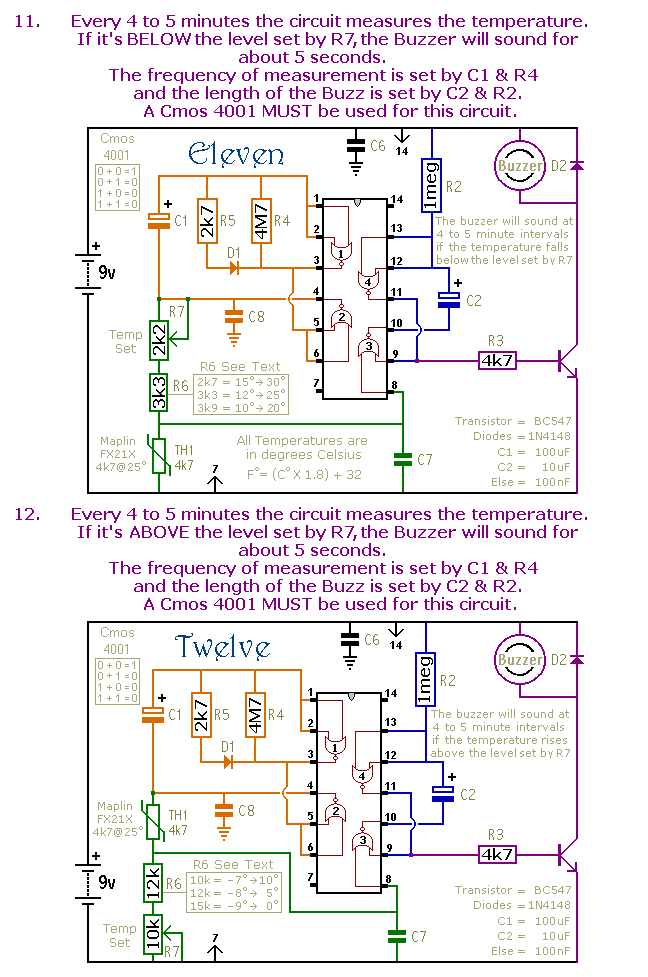
Mini LOGGER V1.0 Block Diagram
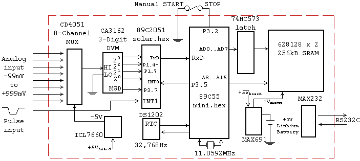
The MiniLOGGER circuit integrates several key components to facilitate its function as a multi-channel data logger. The CMOS analog multiplexer (4051) allows for the selection of one of eight input channels, which are processed as single-ended signals. These signals are then fed into the CA3162 analog-to-digital converter, which is set to operate in free-running mode. The converter outputs a 4-bit Binary-Coded Decimal (BCD) representation of the digital signal, beginning with the Most Significant Digit (MSD) and followed by the Next Significant Digit (NSD) and Least Significant Digit (LSD). The output pulse period for the MSD is specified at 2 milliseconds, ensuring timely data conversion.
The microcontroller, 89C2051, executes the firmware solar3.hex, which orchestrates the reading of the eight channels and manages external pulse reception. When triggered by an INT0 signal, the microcontroller sends the converted digital values via the TxD pin in ASCII format, enabling easy communication with other devices. The 89C55 microcontroller is responsible for reading the data records, which are time-stamped using the DS1202 real-time clock. This data is stored in SRAM and includes date and time information, with channel values separated by commas for clarity.
To enhance the reliability of the MiniLOGGER, a supervisory and power supply chip, MAX691, is integrated to provide battery backup for the SRAM and RTC, ensuring that critical data is retained during power outages. The MAX232 chip is included to facilitate RS232 communication, allowing for connectivity with standard serial devices. Lastly, the ICL7660 negative voltage converter is utilized to generate the necessary negative voltage levels required for certain components in the circuit, ensuring proper operation across the entire system. This comprehensive design enables the MiniLOGGER to function effectively as a robust data acquisition system.A simplified block diagram of the MiniLOGGER is shown in Figure 1. The CMOS analog multiplexer, 4051 provides the output for 8-channel single-end input to an analog-to-digital converter chip, CA3162. The CA3162 is connected in free running mode. The digital output is 4-bit BCD started with MSD, NSD, and LSD. The pulse period of MSD is 2ms. The 89C 2051 runs solar3. hex, the firmware that controls 8-channel reading and receives external pulse. When the chip was triggered by INT0 signal, it will send the digital value in ASCII format through TxD pin; The 89C55 reads such record with time stamped read from DS1202 and saved into SRAM. Now it saves also DATE/TIME and provides comma for each channel separation. There`s also a supervisory and power supply chip, MAX691 for battery backup to SRAM and RTC, MAX232 for RS232 converter, and ICL7660 negative voltage converter.
🔗 External reference
Related Circuits
The IR Theremin hardware schematic is notably simple, as the primary input and output devices require minimal connections. This simplicity can be a double-edged sword, as fewer hardware components often lead to increased software complexity. The main components utilized...
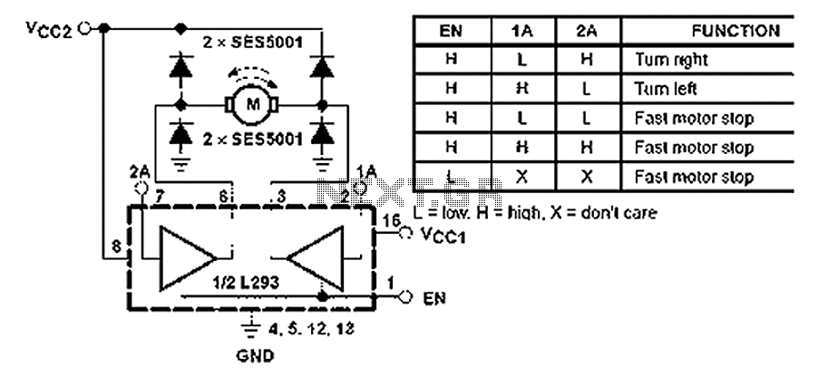
All inputs are compatible with TTL. Each output consists of a complete totem pole driver circuit, utilizing Darlington transistors and pseudo-Darlington sources. The driver enable signals, labeled as 1,2 EN and 3,4 EN, control the activation of drivers 1...
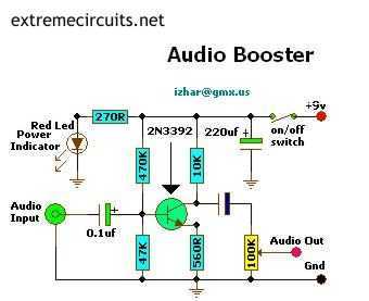
This small amplifier circuit is ideal for boosting small audio units. The small amplifier circuit is designed to enhance the audio signals from low-output devices, such as microphones or portable music players. It typically employs a transistor or an operational...
This is a selection of small self-contained alarm circuits. They have a very low standby current; and are suitable for battery operation. The described alarm circuits are compact and designed for low power consumption, making them ideal for battery-powered applications....
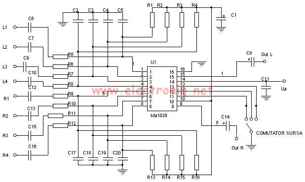
The TDA1029 is a dual operational amplifier configured as an impedance converter. Each amplifier features four mutually switchable inputs that are safeguarded by clamping diodes. Signal sources can be switched in various modes. The electronic components required for this...
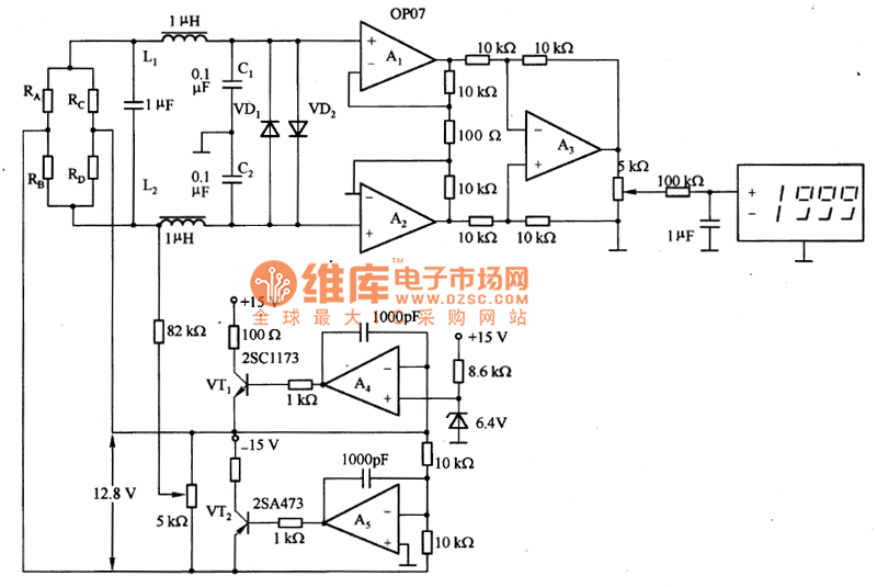
The figure illustrates a digital display pressure measuring circuit diagram. The circuit operates with an additional voltage of approximately 12.8V and draws a current of 30mA. Under maximum gain conditions, the input voltage range is 0.8mV. The zero adjustment...