
Monolithic Synchronous Voltage-to-Frequency Converter
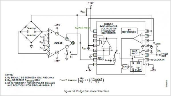
The AD654 voltage-to-frequency converter is designed for a variety of applications where precise conversion of voltage signals into frequency signals is required. The integration of a high-performance input amplifier ensures that the device can accurately process low-level signals, making it suitable for use with sensors such as thermocouples and strain gauges. The precision oscillator system within the AD654 is critical for maintaining accuracy across a wide frequency range, allowing for effective signal conversion up to 500 kHz.
The linearity error of 0.03% at 250 kHz indicates that the device can maintain a high degree of accuracy even at elevated frequencies, making it ideal for precision measurement applications. The 80 dB dynamic range ensures that the converter can handle a variety of input signal levels without significant distortion, making it versatile for different use cases.
Operationally, the AD654 is efficient, requiring only a single supply voltage, which simplifies circuit design and reduces the need for additional components. The low quiescent current of 2.0 mA contributes to overall energy efficiency, making the AD654 suitable for battery-operated devices. The high input impedance of 250 MΩ minimizes loading effects on the input signal, preserving the integrity of the measurement.
Furthermore, the capability to drive multiple TTL loads and optocouplers makes the AD654 an excellent choice for interfacing with digital systems and long-distance signal transmission. The square-wave output feature provides a straightforward means of signal processing, enhancing the versatility of the device in various electronic applications. Overall, the AD654 is a robust and highly functional V/F converter suitable for precision measurement and signal processing tasks in electronic systems.The AD654 is a monolithic V/F converter consisting of an input Amplifier a precision Oscillator system, and a high current output stage. A single RC network is all that is required to set up any full scale (FS) frequency up to 500 kHz and any FS input voltage up to 30 V.
Linearity error is only 0. 03% for a 250 kHz FS, and operation is guaranteed o ver an 80 dB dynamic range. The overall temperature coefficient (excluding the effects of external components) is typically 50 ppm/C. The AD654 operates from a single supply of 5 V to 36 V and consumes only 2. 0 mA quiescent current. The low drift (4 V/C typ) input Amplifier allows operation directly from small signals such as thermocouples or strain gauges while offering a high (250 M(ohm) input resistance.
Unlike most V/F converters, the AD654 provides a square-wave output, and CAN drive up to 12 TTL loads, Optocouplers long cables, or similar loads. 🔗 External reference
Related Circuits
The purpose of this application note is to present an example circuit illustrating the operation of the XR-T5683 device at a data rate of 10.1 Mbps. This note includes the results of measurements taken on the XR-T5683 at this...
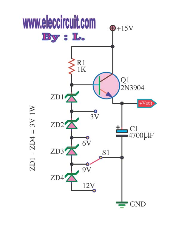
This is a DC regulator circuit that can provide multiple output voltages simply. It functions as a simple step-down DC converter and is designed with a fixed resistor R1. The described circuit operates as a DC voltage regulator, specifically designed...
Both converters utilize CMOS inverters. Figure 105-1A illustrates a free-running circuit where both pulse duration and pulse pause are influenced by the temperature of diode D8. This configuration is suitable for applications where synchronization between the converter and other...
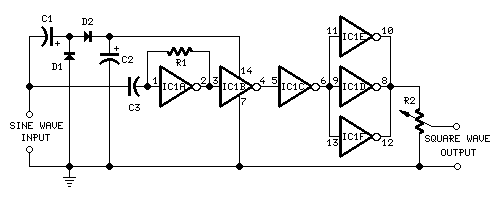
This circuit is designed to generate high-quality square waves by converting a sine wave obtained from an existing generator. A key feature of this circuit is that it does not require an external power source; it can be directly...
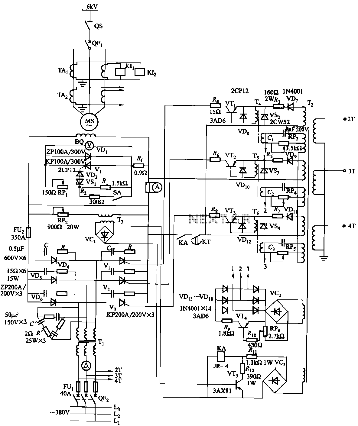
The excitation device for a light-duty synchronous motor rated at 625 kW has been initiated. The triggering circuit of the device consists of three identical RC phase-shift flip-flops. Adjustment potentiometers RP3 to RPs are used to set the RC...
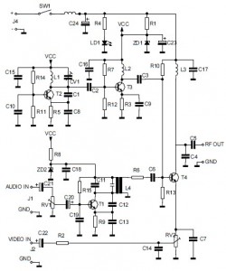
This is the circuit diagram of an audio/video modulator. The circuit converts audio and video signals into a UHF TV signal. It is designed to connect a video signal originating from a camera or other video source to a...