
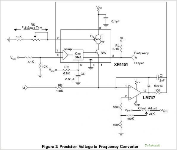
XR4151 XR4151 -Voltage-to-Frequency Converter
The XR-T5683 device is a high-performance integrated circuit designed for digital communication applications. Operating at 10.1 Mbps, this device is capable of handling various data transmission tasks efficiently. The circuit in question utilizes a modified board that was initially intended for a lower data rate of 8.448 Mbps. This modification demonstrates the flexibility of the XR-T5683 in adapting to different operational parameters.
The key adjustment made to the circuit involved the tuning capacitor within the LC clock extraction circuit. The tuning capacitor plays a critical role in ensuring the stability and accuracy of the clock signal, which is essential for synchronizing data transmission. By lowering the capacitor value, the circuit was optimized for the higher data rate, allowing for improved performance and reliability.
Measurements taken during the evaluation provide valuable insights into the operational characteristics of the XR-T5683 at 10.1 Mbps. These measurements include parameters such as signal integrity, jitter performance, and power consumption, which are crucial for assessing the overall functionality of the device in a real-world application. The results confirm that the XR-T5683 can maintain robust performance even when operating at higher data rates, making it suitable for various high-speed communication systems.
Overall, the modifications and subsequent measurements highlight the adaptability of the XR-T5683 device and provide a clear example of how to effectively operate this integrated circuit in high-speed applications.The purpose of this application note is to present an example circuit, illustrating how to operate the XR-T5683 device at 10. 1 Mbps. This note shows the results of measurements made on the XR-T5683 at a 10. 1 Mbps data rate. Hardware used for this evaluation was a slightly modified board designed for 8. 448 Mbps E2 service. The only change to the ci rcuit, which is shown in Figure 1, involved lowering the LC Clock extraction circuit tuning capacitor value. 🔗 External reference
Related Circuits
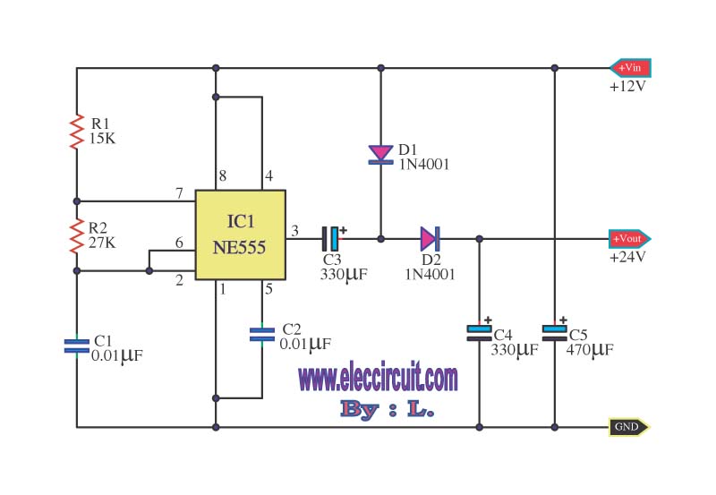
This is a simple voltage doubler circuit that converts 12V DC into 24V DC. It utilizes the popular NE555 timer IC along with a few additional components. The circuit can provide approximately 50mA of current, making it suitable for...

This is a 35.3 to 10.7 MHz converter circuit. It converts the 35.3 MHz signal coming from a VHF/UHF tuner down to an FM tuner to decode the TV audio in FM. The 35.3 to 10.7 MHz converter circuit is...

Normally, an analog-to-digital converter (ADC) requires interfacing through a chip to convert analog signals into digital format. This necessitates both hardware and software, resulting in increased complexity and overall cost. The circuit presented here is configured around the ADC...
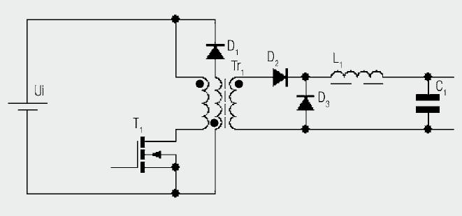
The diagram illustrates the basic construction of a forward converter. In contrast to the flyback converter, which temporarily stores energy before transferring it to the secondary side, the forward converter facilitates direct energy transfer between the primary and secondary...
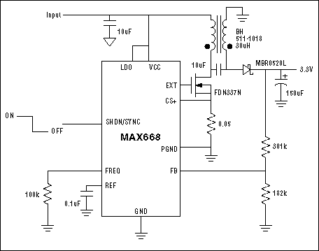
A step-up converter followed by an LDO regulator provides improved battery life compared to a traditional SEPIC design when powered by a single lithium-ion cell. The circuit design features a step-up (boost) converter that elevates the input voltage from a...
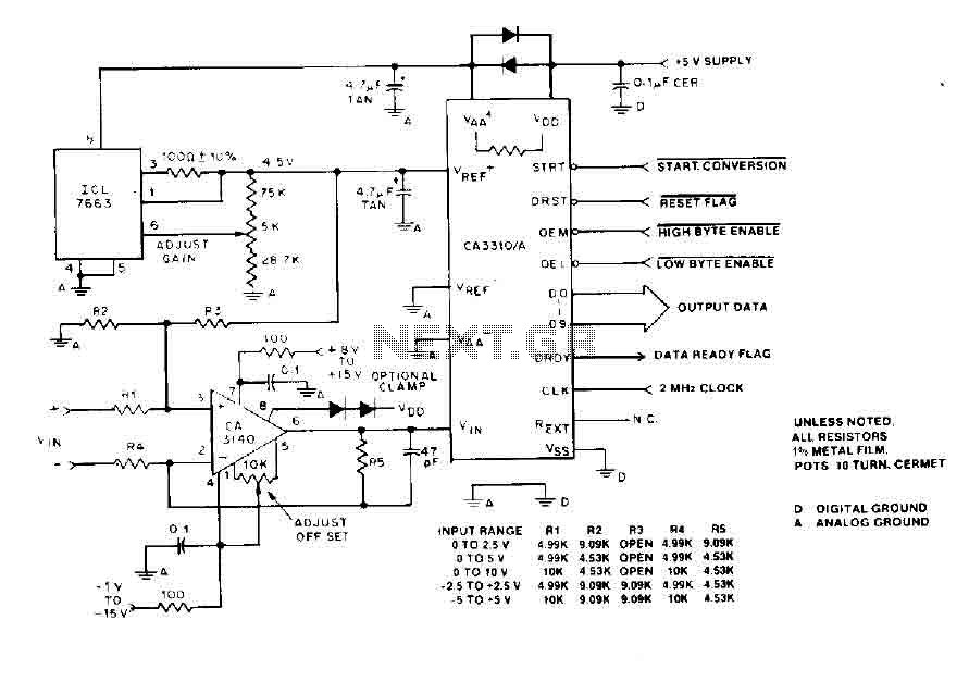
The BiMOS CA3140 operational amplifier offers excellent orientation capabilities for high bandwidth signal inputs and can swiftly adjust the energy output at its terminal CA33IO WINE. The CA3140 can also operate close to the negative supply rail. If the...