
multi channel audio mixer using jfet
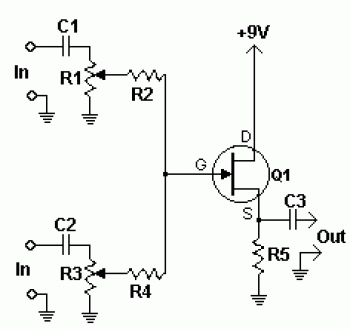
The 2N3819 JFET is optimized for applications requiring high-frequency performance, such as radio frequency amplification and signal mixing. Its low noise characteristics make it suitable for sensitive RF applications where signal integrity is paramount. The device operates with a low gate-source voltage, facilitating its use in low-power circuits.
To fabricate a PCB for a project involving the 2N3819, the following steps provide a clear guide to ensure a successful outcome. First, utilize PCB design software, such as Eagle, to accurately draft the circuit schematic and layout. This software allows for precise component placement and routing of traces, which is essential for maintaining signal integrity at high frequencies.
Once the design is complete, the next step is to print the layout. A laser printer is preferred due to its ability to produce high-resolution prints that are crucial for the transfer process. The printed design should be on photo or glossy paper, as these materials provide better ink adhesion during the heat transfer process. If a laser printer is not available, using standard paper is acceptable, but it may require additional steps to ensure proper transfer.
After printing, the design must be adhered to the copper-clad PCB. This is done by placing the printed side against the copper surface and applying heat with a hot iron plate. The heat causes the toner to melt and bond with the copper, creating a mask for the subsequent etching process. It is crucial to apply even pressure and heat to ensure full coverage and adherence.
Following the transfer, the PCB can be submerged in an etching solution to remove the unprotected copper. This step reveals the circuit traces that will connect the various components, including the 2N3819 JFET. After etching, the PCB should be cleaned and inspected for any defects before proceeding to soldering components.
In summary, the 2N3819 is an excellent choice for RF applications due to its performance characteristics. The PCB creation process outlined provides a clear method for hobbyists and engineers alike to fabricate their own circuit boards, facilitating the implementation of this versatile JFET in various electronic designs.2N3819 is an n-channel JFET especially manufactured for RF and mixer applications and provides very low noise, very low distortion and excellent high frequency gain. Make a PCB in very easy steps. ! Create your PCB design using PCB designer software like Eagle, print out your design on photo paper or glossy paper with laserjet printer.
Stick the pr inted design on the PCB (copper side) and then heat it using hot iron plate. The ink will stick on the PCB and it will be ready for etching process. Note: If you don`t have laserjet printer, then you can print the design on standard paper. Copy the printed design at Copy Service around your location (with glossy paper). 🔗 External reference
Related Circuits
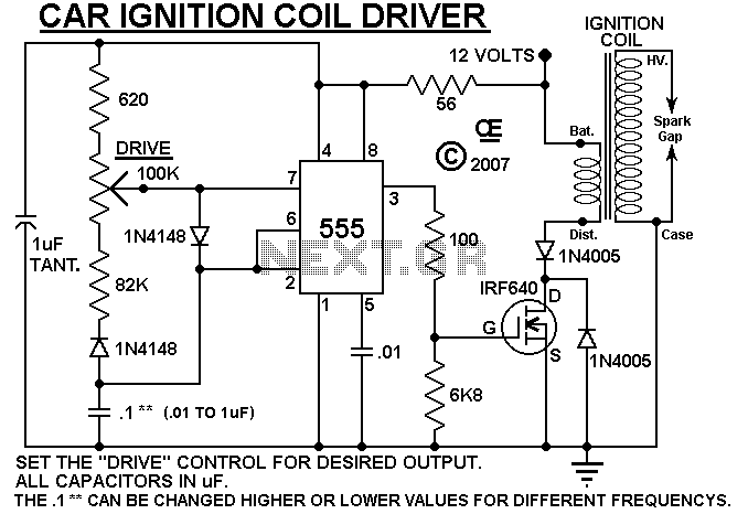
A simple design based on a 555 to drive a car ignition coil. This was designed for a small electric fence to protect a vegetable garden from small animals called marmots. Last year, they ate one of the crops...
This weblog discusses electronic circuit schematics, PCB design, DIY kits, and electronic project diagrams. The subject circuit is a quality preamplifier with a built-in USB DAC designed for the Leachamp power amplifier. The schematic is based on the PCM2902...
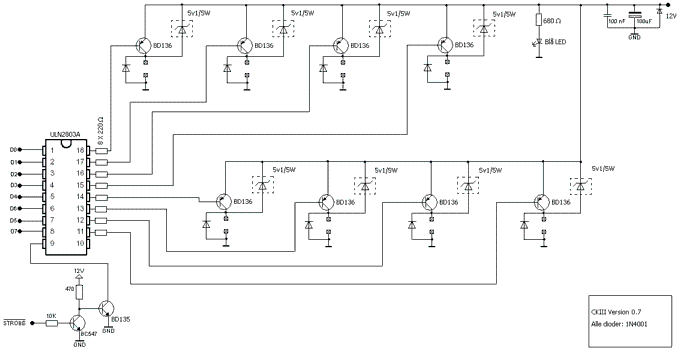
This article was previously published, but the intention is to spread the idea further, potentially inspiring new concepts. An improved version was being developed using an ULN2803A instead of multiple BC547B transistors and optional Zener diodes to ensure that...
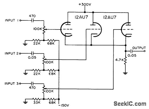
Each grid is biased to cutoff, allowing the mixer to accept only positive-polarity pulses with sufficient amplitude to overcome this bias. -NBS, "Handbook Preferred Circuits Navy Aeronautical Electronic Equipment," Vol. 1, Electron Tube Circuits, 1963, p N4-2. In a typical...
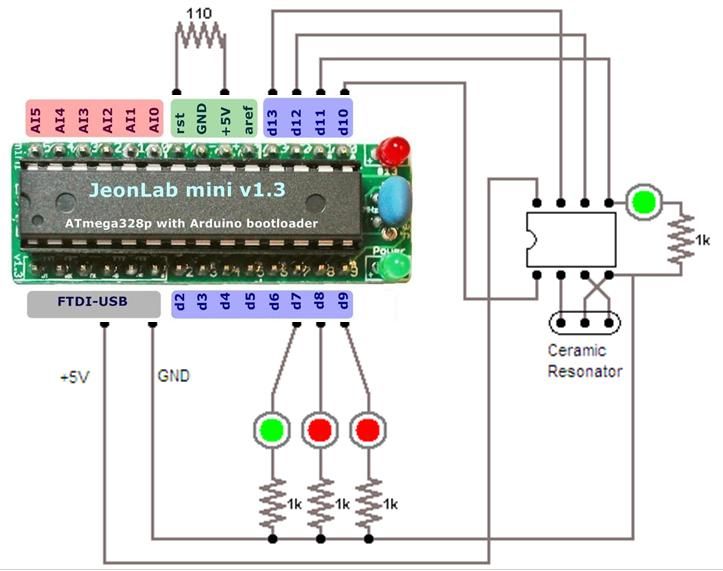
For relatively small projects with fewer pins than the ATmega328, the ATtiny series, specifically the ATtiny45 or ATtiny85, is a good choice due to its compact physical size. The ATtiny series microcontrollers, particularly the ATtiny45 and ATtiny85, are designed for...
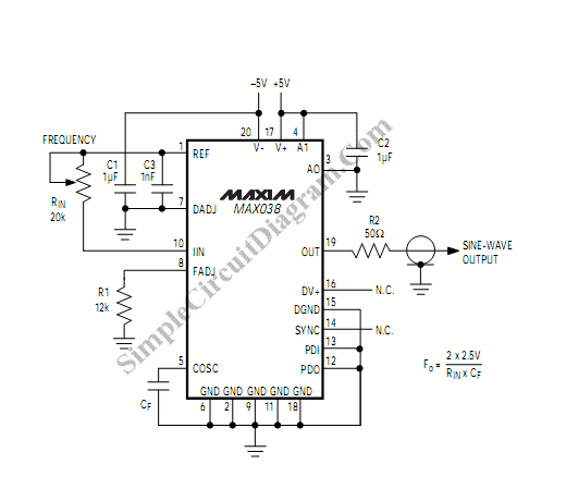
A function generator that operates within a frequency range of 0.1 Hz to 20 MHz can be constructed using the MAX038 integrated circuit chip. This represents a straightforward implementation of a high-performance signal generator. The MAX038 is a high-speed precision...
Warning: include(partials/cookie-banner.php): Failed to open stream: Permission denied in /var/www/html/nextgr/view-circuit.php on line 713
Warning: include(): Failed opening 'partials/cookie-banner.php' for inclusion (include_path='.:/usr/share/php') in /var/www/html/nextgr/view-circuit.php on line 713