
Multi-Purpose VFO
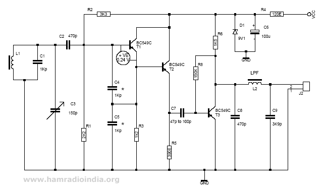
The VFO circuit is fundamentally based on a Colpitts oscillator configuration, which utilizes a combination of inductors and capacitors to establish oscillation at the desired frequency. The circuit typically includes a bipolar junction transistor (BJT) configured in common emitter mode to amplify the oscillation signal. The choice of inductance and capacitance values is critical in determining the oscillation frequency and stability.
To achieve high Q factor performance, careful selection of the inductor winding and capacitor types is essential. The inductor should be wound with minimal stray capacitance and inductive losses, while the capacitors should exhibit low equivalent series resistance (ESR) to maintain stability. The feedback network, which is composed of capacitors connected to the emitter and base of the transistor, plays a crucial role in determining the gain and phase shift necessary for sustained oscillation.
The stability of the VFO can be further enhanced by implementing temperature compensation techniques, such as using thermally stable components or incorporating a temperature-sensitive resistor in the feedback path. This helps mitigate frequency drift caused by temperature variations.
In practical applications, the VFO may be integrated into a larger transceiver design, where its output feeds into mixers or filters for further signal processing. Proper layout considerations, including minimizing lead lengths and ensuring adequate grounding, are essential to prevent unwanted interference and maintain signal integrity.
Overall, a well-designed VFO circuit can provide reliable frequency generation for various amateur radio applications, balancing performance, stability, and ease of assembly for hobbyists. The insights gained from discussions with experienced operators contribute significantly to the development of effective VFO designs.The Frequency instability in VFO stage is a common problem. This is usually occurred in VFO`s due to low Q of the tank circuit, capacitors real value, power supply regulation, stray capacitance, lead inductances and over feed back levels etc. Few months back, I had discussed about VFOs and Oscillators with one of the veteran home brewer, he is
a senior amateur licence holder than me and he is working as JE in communication filed. In that discussion, he told me that while oscillating the bi-polar transistor based VFOs, the first transistor emitter-base voltage should shows as negative volt and this Js an indication of healthy operation. He showed me a practical demo also. When I started my 7MHz, AM/SSB/CW RX project due to heavy compulsion from HAM`S and SWL`s. I started designing work on September 2004, the aim to release the circuits and the PCB on Adoor HAM `XPO 2004 on 21 st November.
I strictly started the proper designing for the benefit of new license holders and SWL`s to get practice about systematic receiver assembling. During that period, while designing the 7 Mhz RX project, I discussed with VU2ARA, Arasu, about VFOs through Kodai VHF repeater.
He strictly told that the first transistor emitter-base voltage must be a positive volt. Due to this positive and negative charge a lightning stroked my brain. VU2ARA never disclosed the exact principle about a positive voltage at emitter-base while oscillating and he forced me to find out myself. I could not get any information from anywhere including ARRL or from any other amateur radio based articles.
I discussed with VU2ITI, Prof. T. K. Mani and he supported the statement of VU2ARA and reminded me that the first transistor is in class A` mode. Then I realised why the positive voltage should keep at E-B junction. In DX articles they are using FETs for stability. But they cannot achieve the goal. I referred colpitts oscillator in electronic principles by Malvino-Mc Graw-Hill, Malvino directly and indirectly stated the parameters and problems of the clopitts oscillator.
I selected the L & C combination in my own way. In general high value inductance with high `Q` is not possible to homebrew, but low inductance with high `Q` is simply possible. I started the VFO work with the basic structure of RM 96 VFO. I got very tremendous performance and the stability of the frequency is just 1Hz tolerance like a DDS.
Now a days everybody going for DDS for getting stability. But this will cost more than Rs. 2, 500. The DDS is very much useful for multi band transceiver project with lot of other features. But for a single band transceiver using DDS is absolutely waste. Then I tested with different inductance combinations for getting different frequencies (refer table). If you are using 2J or 2X gang, connect a series capacitor to reduce the total gang capacitance to get proper spread.
So this modification will give excellent stability for a long duration running. Another beauty of this design is that, you don`t want to use any shielding (there is no temperature influence). The important tip for the stability in a VFO is the emitter base voltage of the first transistor should keep A +ve like 0.
2 to 0. 5V. If it is zero or negative, then the frequency may drift or makes lot of harmonics (Due to change in the amplifier classification - A, AB, B or in C mode). The negative voltage occurs when the feed back level is too high. If I followed the negative voltage principle, stated by the senior HAM friend, then I may have been doing the dig grave of my bi-polar VFO project.
In HAM Radio, thorough experiments, knowledge and discussion will give more flourishing results. In this case VU2ARA guided me in the right way. The L & C combination in this table are evaluated in my shack the inductance former is 10mm, 10 mm based IFT slug can core type which is much popular in RM-96 project. The tank capacitor and the feed back capacitors are 🔗 External reference
Related Circuits
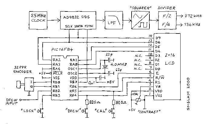
Almost any 2x16 character LCD module with Hitachi HD44780 controller chip will work. The LCD pin numbers on the schematic are not valid for all LCD modules. Please check the actual signal names on your particular LCD module. The...
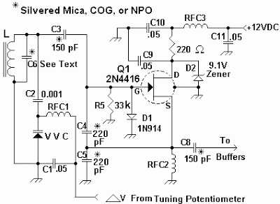
The Colpitts oscillator has been redrawn for clarity. The inductor (L) is approximately 1.5 µH with 19 turns wound on a T50-6 core (yellow). The capacitor (C6) value has been determined experimentally, with a combination of 69 pF (using...
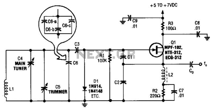
This basic VFO (Voltage Controlled Oscillator) operates within the 3 to 6 MHz frequency range and is commonly utilized in amateur radio applications, employing a Colpitts oscillator configuration. For operation at frequencies between 5 to 5.5 MHz, capacitors C2...
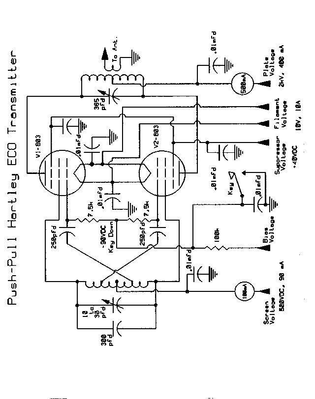
This is a variation of the Electron Coupled Oscillator (ECO) circuit, pioneered by Dow in 1931. Dow's ECO has the screen grounded for RF. In this circuit, filament-type tubes are used instead of heater-cathode types, eliminating the need for...
The three schematics illustrate three building blocks for a 10-meter SSB transmitter. These blocks can also be utilized independently as circuit modules for other transmitters. The VFO board incorporates an FET transmission oscillator, with the VFO signal being mixed...
This document provides the complete schematic for the circuit found on the AMZ Multi-Purpose PC Board. The example circuits do not utilize every component placed on the board; additional parts have been included to enhance flexibility and options. The...