
Multi-Purpose Booster and Buffer
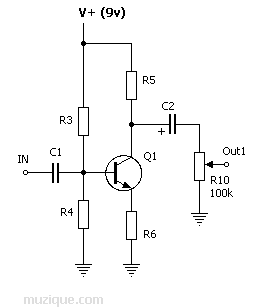
The AMZ Multi-Purpose PC Board schematic is designed for versatility, allowing users to create a variety of electronic projects with minimal modification. The inclusion of extra components provides an opportunity for customization, enabling users to adapt the board for specific applications, including signal amplification and buffering.
The transistor position (Q1) is critical in the circuit design, as it determines the gain characteristics and overall performance. The choice of using a TO-92 or BC108 transistor depends on the desired specifications and the application at hand. Proper orientation of the transistor leads is essential to ensure correct operation; failure to adhere to the specified configurations can result in malfunction.
The optional trimpot at the R5 position allows for fine-tuning of resistance values, which can be beneficial in optimizing circuit performance for various operational conditions. The presence of polarity markings for the capacitors is crucial to prevent damage, as incorrect installation can lead to circuit failure or component destruction.
This schematic serves as a foundational reference for constructing a basic bipolar transistor booster, with the potential for expansion into more complex configurations. The simplicity of the design, combined with the high gain, makes it suitable for a range of applications in audio amplification and signal processing. The external mounting of the R10 potentiometer provides additional flexibility in adjusting output levels without requiring significant alterations to the PCB layout. Overall, the AMZ Multi-Purpose PC Board is a robust platform for experimentation and development in electronic circuit design.This is the complete schematic for the circuit that is contained on the AMZ Multi-Purpose PC Board. None of the example circuits will utilize every part that has been positioned on the board. Extra parts have been included to add flexibility and options to the boards. The basic idea is to create a single pc board that can be used to make multiple projects, including boosters, buffers and more. If a part is not shown on the schematic or in the parts list for one of the circuits, then it is not required for that project and can be left empty on the pcb. The circular object immediately above the "Gr" designation is the transistor location (Q1). It is large enough to accomodate even a TO-5 package. The small tab on the bottom left edge is the indicator for the emitter lead. When using a TO-92 bipolar transistor (E-B-C), it should be oriented with the flat side facing to the right.
This puts the emitter at the bottom and the collector at the top. The base lead will have to be bent slightly to fit in the middle hole. Note that a BC108 style transistor is C-B-E and should have the flat side facing left. Always check your transistor datasheet to find the proper pin designations. There are a few more special items to note on the pc board. First, there is a small circular pad immediately above the printed R3 designation on the board. This pad is only used for a couple of circuits and is ignored the rest of the time. Second, the R5 position has three pads in the middle between the resistor pads. These are for an optional trimpot that is used as the R5 resistor for some circuit variations. If the trimpot is not specified, the pads are ignored and the resistor soldered across the pads above and below the R5 box. Also, polarity signs have been added for C2, C3 and C4; they are not on the pcb. The positive side of electroytics should be oriented to the plus signs as required. These markings are correct for NPN versions and n-fet or n-mos circuits. The circuit shown here is a basic bipolar transistor booster exactly like the ancient LPB-1. It is a simple design with lots of gain. The R10 potentiometer is mounted off the pc board. 🔗 External reference
Related Circuits
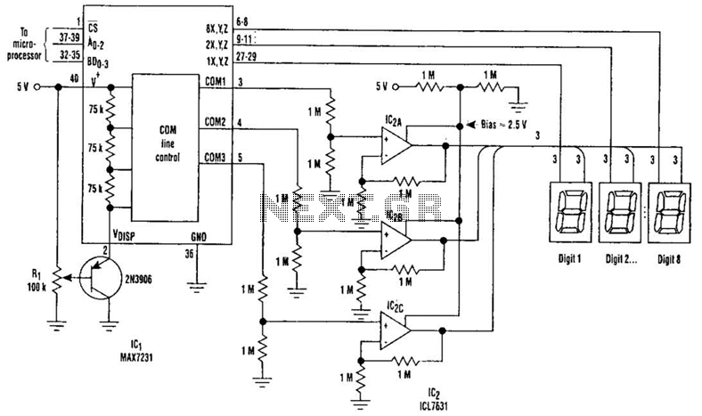
Large LCD devices with one or more displays exhibit significant driving capacitance to the driver circuits. To address this issue, the drive circuit incorporates a buffer amplifier for each of the three common lines. Each amplifier can be programmed...
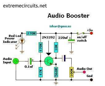
This small amplifier circuit is ideal for boosting small audio units. The small amplifier circuit is designed to enhance the audio signals from low-output devices, such as microphones or portable music players. It typically employs a transistor or an operational...
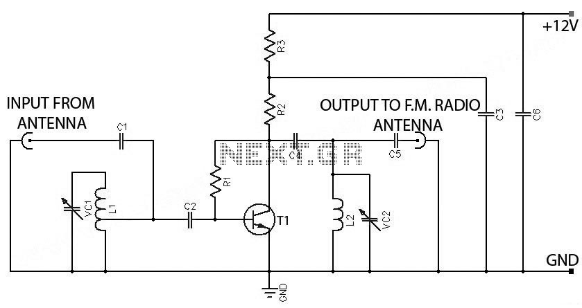
FM Booster, Active FM Antenna Amplifier. This FM booster can be used to listen to programs from distant FM stations clearly. The circuit comprises a common-emitter tuned RF preamplifier wired around VHF/UHF transistor 2SC2570. The FM booster circuit is designed...
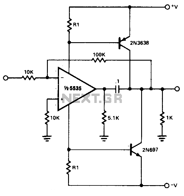
The power booster is designed to drive moderate loads. The circuit utilizes a NE5535 device. Other amplifiers may be substituted, provided that the resistor values (R1) are adjusted according to the Icc current requirements of the chosen amplifier. Additionally,...
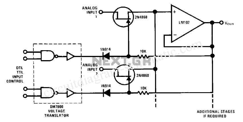
This analog switch utilizes the 2N4860 JFET, which features a low on-resistance (rON) of 25 ohms and minimal leakage current. The LM102 acts as a voltage buffer in the circuit. It is designed to be adaptable for use in...
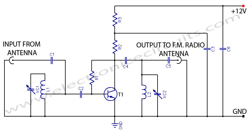
This FM booster allows for clear reception of programs from distant FM stations. The circuit features a common-emitter tuned RF preamplifier utilizing the VHF/UHF transistor 2SC2570 (only labeled as C2570 on the transistor body). The input coil L1 is...