
nixie tube clock circuit
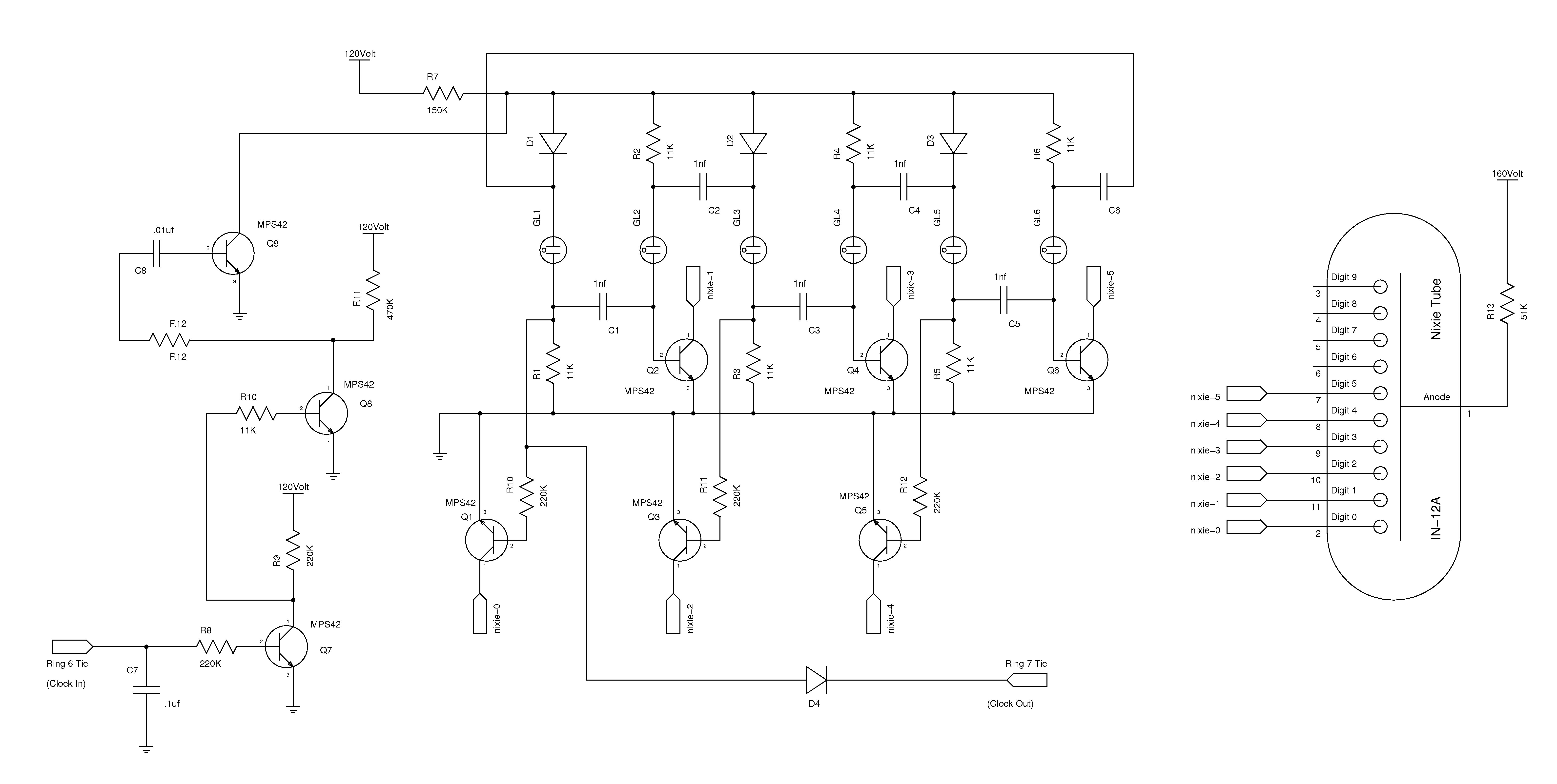
The nixie tube clock design integrates various electronic components to achieve precise timekeeping and display functionality. The high-voltage power supply stage is critical, as it transforms the 12 volts AC input into the necessary 160 volts DC needed for the nixie tube operation. The Maxim 1771 switching regulator plays a vital role in this conversion, utilizing a MOSFET to control the energy transfer to the coil L1. The pulse width modulation (PWM) achieved through the feedback mechanism involving resistors and the potentiometer allows for stable voltage regulation, ensuring consistent performance of the ring counters.
The ring counters, which are pivotal in the timekeeping process, utilize a combination of divide ratios to accurately count time intervals. The division of the incoming 60Hz signal into lower frequencies facilitates the generation of 1Hz pulses, which correspond to seconds, and further divisions yield minute and hour counts. The use of transistors in the triggering circuits enhances the reliability of the pulse generation, ensuring that the timing signals are clean and free from noise, which is essential for the accurate operation of the nixie tubes.
Each ring counter is designed to operate with specific characteristics, with the initial two rings employing a simpler triggering mechanism compared to the more complex configurations used in subsequent rings. The cascading of pulse outputs allows for a seamless transition between the different counting stages, with careful consideration given to the loading effects that could impact performance.
The integration of neon lamps as indicators for the counters leverages their unique electrical properties, where the voltage required to initiate illumination differs from that required to maintain it. This characteristic is exploited to ensure that only one lamp is lit at a time, providing a clear and distinct representation of the current time digit being displayed.
Overall, this schematic design represents a sophisticated approach to building a nixie tube clock, combining high-voltage power management, precise timing circuits, and effective display technologies to create an aesthetically pleasing and functional timekeeping device.The nixie tube clock consists of a high voltage power supply, seven rings counters and an Atmel AVR processor. The power supply is shown in schematic Schematic 1. It takes 12 volts AC and converts it to DC which drives the Maxim 1771 switching power supply to generate 160 volts.
The Maxim 1771 operates by effectively shorting the 12 volts DC to ground through the coil L1 using the MOSFET Q1. When it turns off Q1, this releases the coil from ground and a large positive spike is generated which is then stored in an electrolytic capacitor C3. The diode D1 keeps the capacitor from discharging back though the circuit. Resistors R2, R4 and the potentiometer R3 make a voltage divider which feeds a small voltage back to the Maxim IC so that it can adjust the pulses frequency and duty cycle to regulate the voltage.
Resistor R5 and zener diode Z1 are used to regulate down this down to 120 volts do drive the ring counters. The AC input is also used to provide a 60hz signal to the first ring as well as an interrupt to the processor.
Three of the ring counters divide by 6, 3 others divide by 10 and the last ring divides by 12. The divide by 6 rings and the divide by 10 rings are paired to count the 60hz down to 1hz, the 1hz to 1cpm and the 1cpm to an hourly pulse. Each of the rings are similar. The difference being the trigger circuit is different for the first two rings than the subsequent rings.
The first two rings use a single transistor to drive them, while a 3 transistor circuit is used to provide clean consistent pulses to drive the remaining rings. In addition to the different triggering circuits, the minutes and 10s of minutes rings have half of the diodes replaced with the base emitter junction of a transistor.
Those transistors as well as others are used to drive the digits of the nixie tubes. Schematic 2 is indicative of the divide by 10 rings. It depicts the simpler 1 transistor trigger circuit which is used in the first 2 rings which divide the 60hz down to 1hz. Notice that the transistor is capacitively coupled to the ring driving the positive side towards ground in short pulses.
The ring counters work by relying on the fact that the neon lamps require a higher voltage to turn on than to remain lit. Schematic 2 will be used to explain the operation of the ring. On initially powering up the ring, one (maybe more) lamps will light. We will assume that lamp GL3 is lit. This will put a 5 to 10 volt drop across R3 which will charge C3 to the same voltage through D4. If a positive pulse is applied to "Pulse In" a negative pulse will be applied to the ring counter which should extinguish the GL3.
This will bring the voltage level on the resistor side of C3 to 0 which will force the diode side of the C3 to -5 to -10 volts. As the voltage is re-established on the ring, lamp GL4 will light up first because it will have the additional voltage of the capacitor as an advantage over the others.
Once it lights, it will draw enough current through the 150K resistor R11 to lower the voltage on the ring down below the level that any of the other lamps will be able to light. The lighting of lamp GL4 will then charge C4 and the process will continue with each pulsing of "Pulse In".
To cascade rings, "Pulse Out" can be taken from the lamp side of any of the 11K resistors which are tied to ground. It must not be loaded too heavily by the successive stage or its operation will be effected. One important thing to remember, as far as the overall nixie clock is considered, the stage which is used for "Pulse Out" will be 0 for that ring.
This is most important for the minutes and 10s of minutes rings. Schematic 3 is indicative of the divide by 6 rings. It depicts the more complex 3 transis 🔗 External reference
Related Circuits
A circuit designed to operate within a frequency range with an accuracy greater than 2% for generating Bode plots. It converts two sine waves into a square wave, taking into account the overlap relative to the total input wave...
The circuit depicted in the figure includes the ISO124 and MC78L05 components, along with an external regulator, MC79L05, and the DCP011515, which collectively enhance the power supply rejection ratio (PSR) of the circuit. The input signal, VIN (maximum swing...
This car audio amplifier circuit is based on the LA47536 audio amplifier integrated circuit designed by Sanyo. This audio amplifier circuit is specifically designed for car audio power amplifiers. The LA47536 car audio amplifier IC features four output channels...
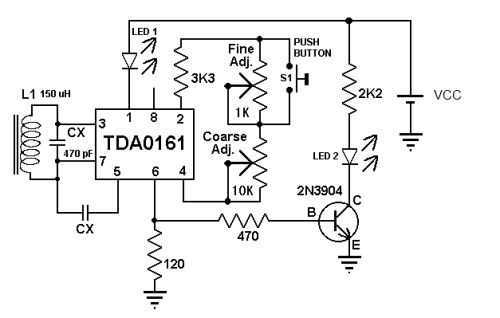
These metal detector circuit diagram is based on the TDA0161 monolithic integrated circuit, designed for metallic body detection by detecting the variations in high frequency Eddy current losses. For detecting metals, TDA0161 require an external LC tuned circuit. Output signal...

Using a Thomson TEA2025, this stereo amplifier delivers 1 W per channel into a 4-ohm load with a 9-V supply. The input sensitivity is 25 mV peak-to-peak for full output. It is important to ensure that pins 4, 5,...

Most thefts occur after midnight when individuals enter the second phase of sleep known as 'paradoxical sleep.' Here is an energy-saving circuit that causes... An energy-saving circuit designed for security applications can be particularly beneficial during the late-night hours when...
Warning: include(partials/cookie-banner.php): Failed to open stream: Permission denied in /var/www/html/nextgr/view-circuit.php on line 713
Warning: include(): Failed opening 'partials/cookie-banner.php' for inclusion (include_path='.:/usr/share/php') in /var/www/html/nextgr/view-circuit.php on line 713