
OCL power amplifying circuit

In the positive half-cycle of the input signal, the output signal also exhibits a positive half-cycle, during which transistors VT4 and VTs conduct while VT6 and VT7 remain off. If the input signal is sufficiently strong, a positive signal peak can cause VTs to approach saturation, resulting in a voltage drop across the output. If the signal is disregarded, the output voltage during the positive peak is influenced by the load resistance Rl4, with the output voltage reaching a maximum value of V+. Conversely, during the negative peak of the input signal, the output voltage corresponds to a negative peak value. Consequently, the maximum output voltage distortion peaks at 2V. When the input signal is sinusoidal, the maximum power output is determined by the equation Pmax = V+^2 / (2 * RLo). In this scenario, the output power is compared to PE = V+^2 / (r * RLo), allowing for the calculation of circuit efficiency, which is determined to be approximately 78.5%.
This OCL power amplifier circuit is designed to provide high efficiency and low distortion in audio applications. The use of a quasi-complementary output stage allows for improved linearity and reduced crossover distortion, making it suitable for high-fidelity audio amplification. The negative feedback mechanism plays a crucial role in maintaining stability and linear gain across varying load conditions. Additionally, the symmetrical power supply configuration ensures that the amplifier can handle both positive and negative signal excursions effectively, contributing to the overall performance and reliability of the circuit. Proper biasing and component selection are essential for achieving optimal performance, particularly in high-power applications where thermal management and signal integrity are critical.Figure 1-30 is an example of an OCL power amplifier circuit, the following specific analysis: In Figure 1-30, VTi, VTz form a single-ended input and differential input single-e nded output amplifier circuit. Signal from the input pole base VTi, VTi from the mother VT3 collector output level to promote, it is by a PNP transistor consisting of a total of hair emitter amplifier circuit, where the use of the PNP and pre-conjugated to the NPN tube adapter, easy midpoint voltage of dying oVT4, VTs and VT6, VT7 composition of the composite quasi-complementary class AB push-pull power output stage. f) 1, f compliance with the islands push-pull output stage quiescent bias circuit, the output stage in class AB, the island can adjust its operating point adjustment.
R: r is negative feedback resistor for adjusting the gain of the circuit and the static stability midpoint voltage VD. Machine with a V + and V two symmetrical power, the output signal symmetry. Shown in Figure 1-30, in the positive half cycle of the input signal, the output signal is positive half cycle o At this time, VT4, VTs lead pass, VT6, VT7 off.
As long as the input signal is strong enough, you can make when you enter a positive signal peak, VTs approaching saturation and the region, which pressure drop is V mouth. If the signal is ignored Rl4 drop on the output signal of the positive peak voltage v + a 1vais :: : V ~ Similarly, when the input signals negative peak, negative peak output signal voltage is aiming V V ten V a.
Therefore, the circuit output voltage distortion maximum peak value of 2V. If the input signal is sinusoidal crossing, the maximum does not lose the power Ponr-ax y + 2/2RLo In this case, the power source output as compared to PE V + 2/rRLo the two values, in order to calculate the efficiency of the circuit Kun 78.5%.
Related Circuits
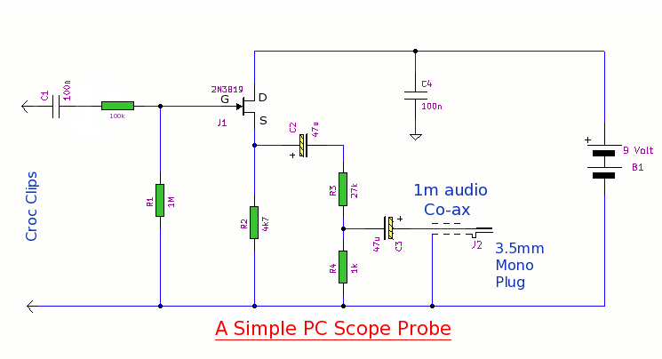
This simple PC scope probe functions as a FET follower, featuring high input impedance and low output impedance to match a microphone or line input socket on a PC or laptop. This design allows for practical examination of waveforms...
After searching for a few days, a solution for this idea has not been found. A switch panel is being created in the dashboard containing four switches. The switch panel design for the dashboard involves integrating four switches that can...
This cell phone charger circuit diagram electronic project is based on the FSEZ1307 third-generation primary side regulation (PSR) PWM controller integrated circuit. The FSEZ1307 cell phone charger can be used for battery charger applications for devices such as cellular...
The LM380 is a power audio amplifier designed for consumer applications. To minimize system costs, the gain is internally fixed at 34 dB. It features a unique input stage that allows for ground-referenced input signals. The output automatically self-centers...
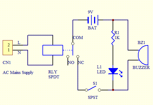
Construct a basic power failure alarm monitoring system utilizing an AC relay that activates a buzzer when the mains power supply is interrupted. The proposed power failure alarm monitoring system is designed to provide an audible alert during a loss...

A series of LEDs is used to alert the gardener when plants require watering. By utilizing two conventional digital integrated LEDs along with a series of additional LEDs, this device serves as a practical tool for gardening. It detects...
Warning: include(partials/cookie-banner.php): Failed to open stream: Permission denied in /var/www/html/nextgr/view-circuit.php on line 713
Warning: include(): Failed opening 'partials/cookie-banner.php' for inclusion (include_path='.:/usr/share/php') in /var/www/html/nextgr/view-circuit.php on line 713