
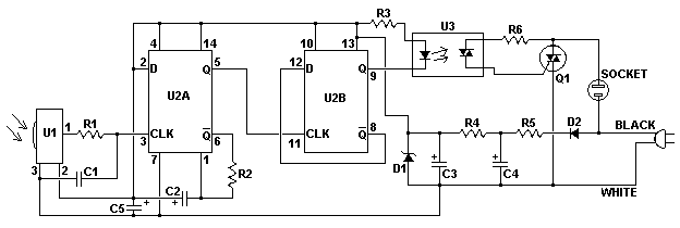
Cell phone charger circuit diagram FSEZ1307
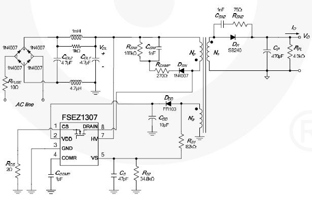
The FSEZ1307 integrated circuit serves as the core component in the design of a compact and efficient cell phone charger. Its primary side regulation architecture eliminates the need for an opto-isolator and secondary feedback, simplifying circuit design and reducing component count. This makes the charger not only cost-effective but also reliable for various portable electronic devices.
The circuit operates in two primary modes: constant voltage (CV) and constant current (CC). In CV mode, the charger maintains a steady output voltage suitable for charging lithium-ion batteries, while in CC mode, it provides a controlled current to prevent overcharging. This dual functionality ensures compatibility with a wide range of battery chemistries and charging requirements.
Key features of the FSEZ1307 include low standby power consumption, which is particularly important for energy efficiency and compliance with modern energy standards. The high-voltage startup capability allows the charger to initiate operation without requiring a separate startup circuit, further simplifying the design.
The fixed PWM frequency of 50 kHz, combined with frequency hopping, helps to minimize electromagnetic interference (EMI), a critical consideration in consumer electronics. Additionally, the built-in cable compensation feature adjusts the output voltage based on the length and resistance of the charging cable, ensuring optimal charging performance.
Safety features such as cycle-by-cycle current limiting protect the circuit from overcurrent conditions, while VDD over-voltage protection and under-voltage lockout mechanisms safeguard against voltage fluctuations that could damage the charger or connected devices. The gate output voltage clamping at 15 V prevents excessive voltage from reaching the power MOSFET, enhancing the reliability of the circuit.
In summary, the FSEZ1307-based cell phone charger circuit diagram represents a modern solution for efficient and safe battery charging, suitable for a variety of electronic devices. Its integration of multiple protective features and operational modes makes it a versatile choice for designers seeking to develop reliable power supply solutions.This cell phone charger circuit diagram electronic project is based on the FSEZ1307 third-generation primary side regulation (PSR) PWM controller integrated circuit. The FEZ1307 cell phone charger can be used for battery chargers applications for devices like : cellular phones, cordless phones, PDA, digital cameras or for replacement of linear tr
ansformers and RCC SMPS. The FEZ1307 is designed to work using few external components offering many other features like : low standby power: under 30mW, high-voltage startup, constant-voltage (CV) and constant-current (CC) control without secondary-feedback circuitry, fixed PWM frequency at 50kHz with frequency hopping to solve EMI problem, cable compensation in CV mode, peak-current-mode control in CV mode, cycle-by-cycle current limiting, VDD over-voltage protection with auto restart, VDD under-voltage vockout (UVLO), gate output maximum voltage clamped at 15V, fixed over-temperature protection with auto restart. 🔗 External reference
Related Circuits
This page outlines how to create a simple theft deterrent that can be quite effective. The concept involves using a flashing red LED to indicate that the vehicle is protected. This device serves to safeguard the car from potential...
After each zero electromagnetic pickup receives a sine wave input, as illustrated in the National Semiconductor LM2907 circuit, it generates an output pulse. This circuit can be utilized in digital control systems. The width of each pulse corresponds to...
The following circuit illustrates an Alarm Power Supply Circuit Diagram. Features include a 1-amp current output, suitable for a Modular Burglar Alarm operating at 12 volts. The Alarm Power Supply Circuit is designed to provide a stable and reliable power...
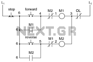
This is the power diagram for motor forward and reverse operation. To change the motor direction, one polarity must be altered, for example, changing R to S. For detailed information, please refer to the following. The described power diagram illustrates...
This circuit allows for the control of any line-powered electrical device, such as a lamp, television, or fan, using any infrared remote control. Many individuals possess a collection of old IR remotes from appliances that are no longer in...
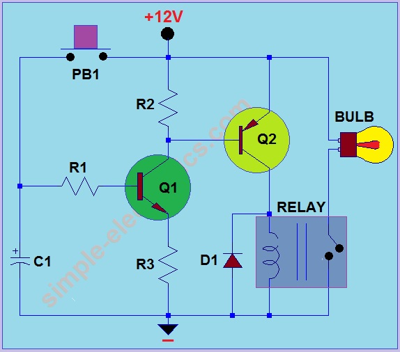
This circuit operates by activating a headlight when the push-button PB1 is pressed. The headlight remains illuminated for a predetermined duration, which can range from several seconds to minutes, before automatically turning off. When PB1 is engaged, capacitor C1...