
Op Amp Regulator
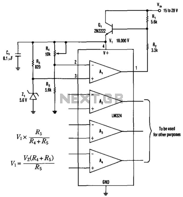
This circuit utilizes an operational amplifier (op-amp) configured to create a stable voltage source with single-polarity output, suitable for various applications requiring consistent voltage levels. The design includes key components: an op-amp (A1), a transistor (Q1), several resistors (R1, R2, R3, R4, R5), and a zener diode.
The operation begins with the transistor Q1 being driven into conduction by the base current supplied through resistor R1. This conduction allows for the establishment of voltage Vi across the supply pins of the op-amp. The configuration of A1, R2, and Q1 forms a positive feedback loop, which is crucial for the initial voltage amplification. Resistor R3 and the zener diode play a critical role in stabilizing the output voltage by limiting the maximum voltage to prevent damage to the circuit components.
The negative feedback mechanism is facilitated by R4 and R5, which work in conjunction with A1, R2, and Q1 to regulate the output voltage. The interaction between the positive and negative feedback loops ensures that the circuit can respond dynamically to changes in load or input conditions. The non-inverting input receives the voltage Vx, while the inverting input is kept at a lower voltage until the zener diode becomes active.
When the voltage at the inverting input exceeds that at the non-inverting input, the output of A1 decreases the base current to Q1 through resistor R2. This action reduces the voltage Vi, thus preventing the output from exceeding the desired level. The circuit will stabilize at a point where the feedback loops balance each other, achieving a steady state that can source more than 30 mA, making it suitable for powering various electronic devices or circuits that require a reliable voltage source.
Overall, this operational amplifier circuit design exemplifies effective voltage regulation through feedback mechanisms, ensuring stable performance in applications demanding consistent voltage levels. This op amp offers a straightforward method of developing a single-polarity stable voltage source (see the figure). TVansi stor Ql gets a base drive through resistor Rl, and conducts to develop a voltage (Vi) across the IC"s supply pins. Amp Al, R2, and Ql form a positive-feedback closed loop, along with R3 and the zener diode. Al, R2, and Ql also form a negative-feedback closed loop with R4 and R5. The effect of positive feedback is predominant as the noninverting input receives Vx while the inverting input receives only: This happens until the zener comes into play.
When the voltage at the inverting input exceeds the voltage at the noninverting input, Al"s output takes away Ql"s base current through R2, which reduces Vi. Hence, an equilibrium condition is reached. Now: This circuit can source more than 30 mA. 🔗 External reference
Related Circuits
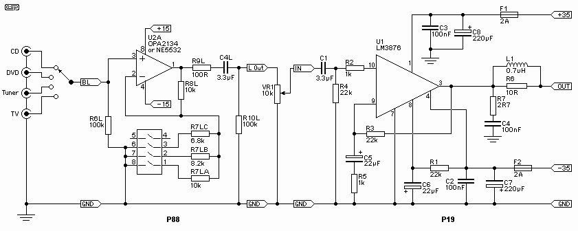
The GainClone concept appears to have gained considerable traction. There are several compelling reasons for this, and I found myself in a situation where SWMBO (She Who Must Be Obeyed) was becoming increasingly agitated as I added amplifiers and speakers...
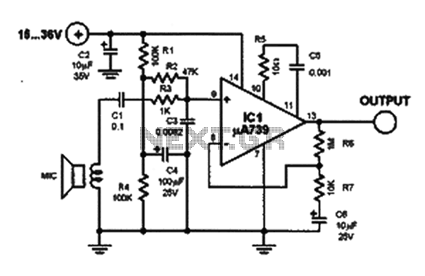
This microphone preamplifier utilizes the low-noise integrated circuit (IC) uA739. It serves as a practical example of designing an effective preamplifier for dynamic microphones. The IC contains two identical integrated preamplifier circuits, with the second preamp functioning in the...
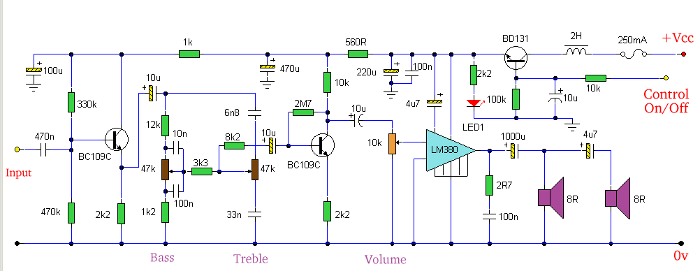
Amplifier with tone controls and soft switching. Notes: The soft switching is enabled by a BD131 transistor configured as a switch in an emitter follower arrangement. The collector is connected to a permanent load. The described amplifier circuit incorporates tone...
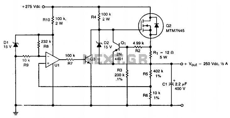
A TMOS MTM7N45 (Q2) is utilized as a series pass element in a linear high voltage supply that accepts +275 V unregulated and produces 250 V regulated with foldback current limiting. A 15 V zener diode (D1) provides the...

In an audio amplifier, the quality of sound depends on several factors, including the quality of active and passive components, circuit configuration, and layout. The selection of components is influenced by the constructor's budget. Discrete active components like transistors...
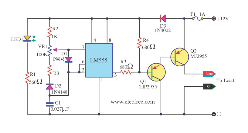
This circuit is a DC dimmer circuit that utilizes the LM555 integrated circuit configured as an astable multivibrator. It is capable of adjusting the duty cycle by fine-tuning variable resistors VR1 and VR2. The DC dimmer circuit employs the LM555...