
Op Amp Stereo Amplifier
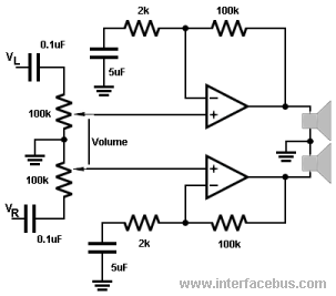
The circuit design features a dual ganged 100k potentiometer, which serves as a volume control for an audio application. This configuration allows simultaneous adjustment of both channels, enhancing user experience by maintaining a balanced audio output. The choice of an audio-taper potentiometer is critical, as it provides a logarithmic response suitable for audio signals, ensuring that volume changes are perceptually uniform across the range of motion.
When integrating operational amplifiers, the selection between individual and dual packages must consider factors such as power dissipation and layout efficiency. The 741 and TL082 Op Amps are frequently utilized due to their established performance characteristics. It is imperative to adhere to best practices regarding power supply decoupling; the bypass capacitors mitigate noise and stabilize the power supply, which is crucial for maintaining signal integrity in audio applications.
The circuit can be further enhanced by incorporating tone controls, which enable the user to tailor the audio output to their preferences. A bass control circuit can be placed before the volume control to ensure that low-frequency adjustments do not affect the overall gain structure. Similarly, a treble control can be added, although combining both into a single tone control can simplify the design while still providing adequate audio customization.
In scenarios where additional speakers are introduced, crossover circuits become essential for directing the appropriate frequency ranges to the respective drivers. This ensures optimal performance across the audio spectrum. The design must also accommodate DC offset considerations, particularly when using a single supply, necessitating the inclusion of coupling capacitors to protect the speakers from unwanted DC levels.
In summary, the described circuit design effectively utilizes ganged potentiometers, operational amplifiers, and optional tone controls to create a versatile audio amplification system, with considerations for power supply stability and speaker protection integrated into the overall schematic.The 100k potentiometers set the voltage level reaching the Op Amps. A dual ganged 100K-Ohm audio-taper potentiometer should be used over a linear taper or potentiometer. In some cases the component may be called a ganged stereo taper. The schematic does not show pin numbers for the Op Amps because the circuit works for either a single or dual package
Op Amp and of course a large number of different Op Amps. However to the right, some different pin numbering is shown. Note that [although not shown well] the two potentiometers are ganged together, one knob changes both potentiometers at the same time. So although each channel uses a different potentiometer they both move up or down at the same time producing a volume control.
A separate balance control could also be added to change the volume of one channel, while reducing the other. Or a separate potentiometer could be added into each channel so that each channel would be adjusted up or down, with regard to the other.
The amplifier could be constructed of either two individual Opamps or a package containing two Op Amps. The 741 is an example of a common Opamp having a single device within the package. Another common example would be a TL082 which is a component with two separate devices within the same package.
The pin functions for both devices are shown the the right. Having two devices in the same package saves parts and and cost. However power dissipation is reduced by having two semiconductors operating in the same package, so a dual op-amp package may not be the way to go. Regardless of the Op Amp used or the number of devices in a package, always bypass the power pin Vcc [Vs, V+] to ground using a.
01uF capacitor [at a minimum]. Bypass capacitors are not shown in many of these schematic diagrams to make them less complicated to read. However it should be understood that by-pass capacitors are always used between all power pins and ground, and in some cases between differential power pins.
Note that in some of these circuits the Op Amp has the inverting input at the top of the component diagram while in other cases the inverting input is below the non-inverting input. Its standard practice to rearrange the input or output pin locations in a schematic diagram to make the schematic easier to read or less complicated.
Most CAD tools allow different versions of a part with different pin locations. When using a split power supply the output of the Op Amp may drive the speaker directly. Basically because the output of the Op Amp normally sits at zero volts, mid-way between to two supply rails. However a capacitor should be connected between the output of the Op Amp and the speaker when a single supply is used.
The capacitor prevents any DC off-set developed by the Op Amp from reaching the speaker. A typical capacitor value may be 205uF. A Cross-over could be added to both the right and left channels so that additional speakers could be added. Even without separate speakers for base and treble, a single base control could be added to the circuit before the volume controls.
In addition a treble control control could also be added. The circuit could be added after the volume control, but normally there are not separate controls per channel. However to reduce complexity a tone control could be used instead of implementing both a base and treble control.
A less complex loudness control might also be added to support the volume control instead of using a base control. Note a few of these circuits are represented as single channel, so they would have to be adapted to two channels.
🔗 External reference
Related Circuits
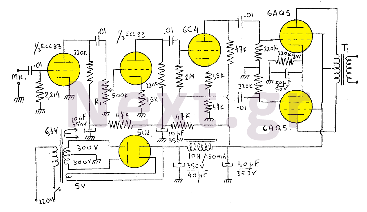
The output of this modulator consists of two 6AQ5 lamps arranged in a push-pull configuration with a maximum output of 15W. A 6C4 lamp is employed as a reversing lamp. The double-stage ESC83 serves as the pre-amplifier. The potentiometer...
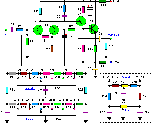
To complement the 60 Watt MOSFET audio amplifier, a high-quality preamplifier design was necessary. A discrete components topology utilizing ±24V supply rails was selected, with an emphasis on minimizing the transistor count while achieving low noise, very low distortion,...
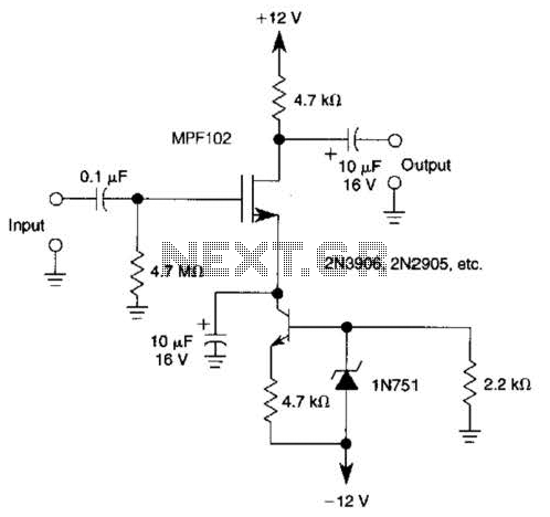
A current source (MPF102) in the source lead of the bipolar transistor 2N3906 allows for precise control of drain current. The circuit incorporates an MPF102 JFET configured as a current source, which is connected to the source terminal of a...
Signal clipping is typically avoided in most applications; however, there are specific instances in audio processing where clipping is intentionally utilized for beneficial effects. Signal clipping is a phenomenon that occurs when an audio signal exceeds the maximum amplitude that...
This circuit consists of a single transistor functioning as an amplifier, providing significant amplification for weak and unipolar signals, which can then be fed into a more powerful amplifier. The described circuit utilizes a single transistor in a common-emitter...
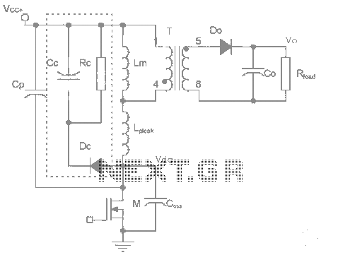
The work process analysis circuit diagram illustrates the use of a flyback converter transformer model. The flyback transformer primarily consists of ideal transformer magnetizing inductance and leakage inductance components. The flyback converter circuit exhibits high-frequency resonance at both ends...