
op amp summer as a digital to analog converter dac
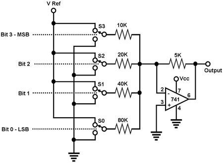
The described circuit utilizes an operational amplifier in a summing configuration to convert digital signals into an analog voltage. The resistors connected to the input serve to weight the binary inputs appropriately, allowing for the conversion of a 4-bit binary number into a corresponding voltage level. Specifically, the resistors are selected to provide weights that correspond to the binary values: 10K for the most significant bit (S3), 20K for the next bit (S2), 40K for the third bit (S1), and 80K for the least significant bit (S0).
The output voltage is determined by the weighted sum of these inputs, which is inverted due to the inverting configuration of the op-amp. The reference voltage (VRef) plays a crucial role in setting the maximum output voltage level. By manipulating the binary inputs, the output voltage can represent any value between 0V (when all inputs are low) and -VRef (when all inputs are high).
To extend the functionality of this DAC, additional switches and corresponding resistors can be integrated into the circuit, allowing for an increased number of bits. This scalability makes it a versatile solution for various applications in digital signal processing, where converting digital signals into analog voltages is necessary. The design emphasizes simplicity and effectiveness, making it suitable for educational purposes and practical implementations in embedded systems.The circuit shown in Figure 1 is a simple 4-bit digital-to-analog converter. It is actually just a simple op amp summer circuit, i. e. , an operational amplifier configured to output a voltage that is proportional to the sum of the input voltages. The op-amp summer circuit above works as a DAC because its input voltages are binary weighted with resp
ect to each other, as set by the resistors (10K, 20K, 40K, 80K) at the inputs. Vo = -VRef (5K) (S3/10K + S2/20K + S1/40K + S0/80K) = -VRef (S3/2 + S2/4 + S1/8 + S0/16) wherein S3, S2, S1, and S0 are the logic inputs (`1` or `0`). The number of bits of this DAC may be increased by connecting more switches with corresponding binary-weighted resistors to the inputs.
🔗 External reference
Related Circuits
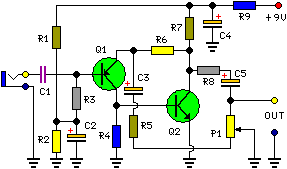
This circuit is primarily designed to provide a microphone input for standard home stereo amplifiers. Utilizing a battery supply effectively eliminates the risk of low-frequency hum interference from mains power, simplifying the connection to the amplifier by removing the...
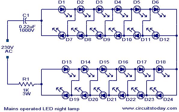
A simple and effective LED-based night lamp circuit is designed to operate directly from the 230V mains supply. The circuit utilizes a total of 24 white LEDs, producing an output of approximately 15W. Current limiting is achieved through resistor...
The proposed scheme is straightforward, requiring only a few external electronic components, making it suitable for car audio construction. The output power ranges from 2 to 4 Ohms, providing 2 x 30 W (with a maximum of 2 x...
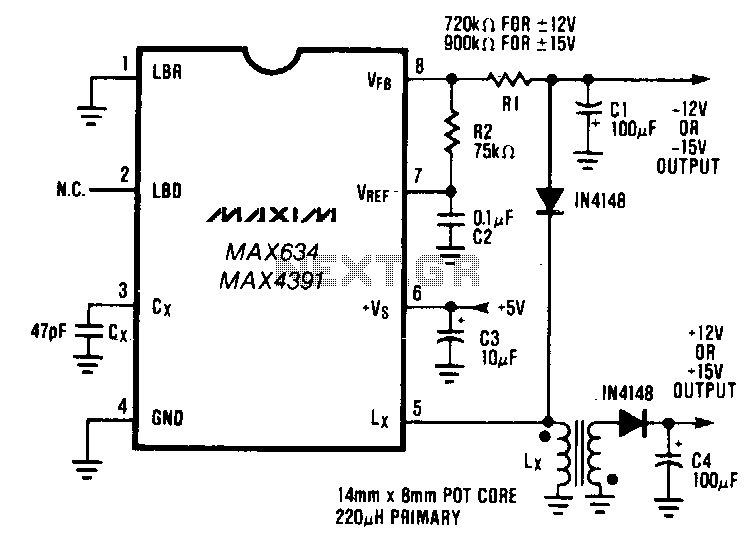
The buck-boost configuration of the MAX634 is well suited for dual output DC-DC converters. Only a second winding on the inductor is needed. Typically, this second winding is bifilar; the primary and secondary are wound simultaneously using two wires...

The genesis for this hybrid electrostatic headphone amplifier occurred when I was in Hawaii on vacation, at a fancy hotel on Maui. Sitting at the bar on the beach, drinking "Blue Hawaiis," I drew the schematic for the amp...
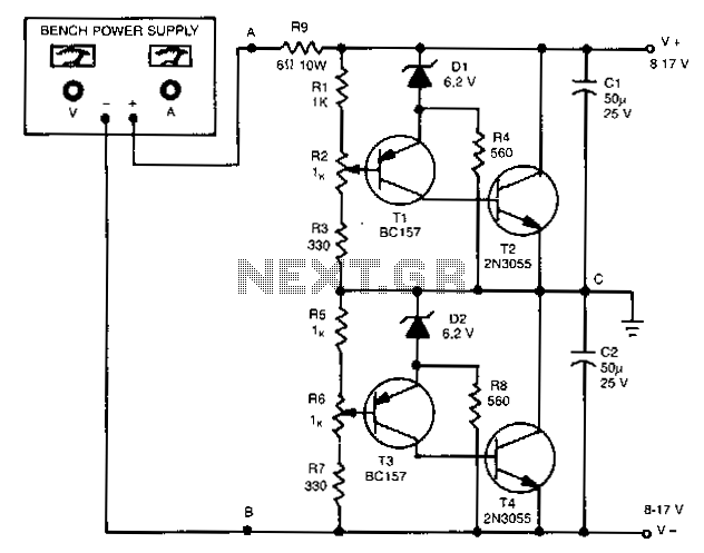
The outputs in this circuit are independently variable and can be loaded unsymmetrically. The output voltage remains constant, regardless of load and changes. By varying potentiometers R2 or R6, the output voltages can be conveniently set. Outputs can be...