
Hybrid Electrostatic Amplifier

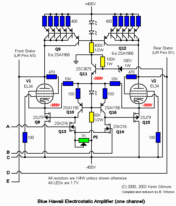
Because the amp is totally DC coupled from input to output, drift in the input stage is a bad idea. Since the first two stages run in current mode, the JFET input is more linear than a pair of bipolar transistors. Dual transistors all on one wafer suitable for audio use are hard to find these days. The FETs steer current away from the current sources Q2 and Q3. Together Q2 and Q3 each supply 2mA or a total of 4mA. The Q17 current source takes away 3mA leaving 0.5mA in each of Q4 and Q5, but some of the sink current is coming from the output feedback, so each FET is actually using somewhere between 0.5mA and 1mA.
The approximate voltage gain of this stage is 5; this stage really runs in current mode. The unit was designed to work equally well in both balanced and unbalanced mode. For single-ended signals, ground either the + or - input and apply signal to the other. The much higher impedance of the JFET works better when one side is grounded for unbalanced inputs.
The second stage starts with a constant current source (Q2 and Q3). The current source feeds a common base amplifier (Q4 and Q5). The common base amplifier feeds a modified Vbe multiplier. I believe a famous designer is now calling this circuit a current tunnel. It's the most linear way of translating the voltage down to the bottom rail. The voltage gain of this section is about 4. The basic idea of the first two stages is to supply the third stage with a very fast low impedance drive signal that is referenced to the bottom rail.
The currents flowing into the common base amplifier (Q4 and Q5) are the difference between what Q2 and Q3 are supplying and what the FET is taking away. The rest of the current goes down the tunnel to the vbe multipliers (Q6 and Q7) that convert the current back to voltage. The current sources in the second stage supply 2 mA each. With no signal, the FETs take 1 mA, leaving 1 mA going through the common base amplifier into the bottom transistors, which are wired as Vbe multipliers (like a zener diode in series with a resistor, except a lot less noisy). This generates the 13 volts (referenced to - rail) necessary to properly bias the third stage.
The third stage is another differential amplifier (Q13 and Q14) being driven via another constant current source (Q10 and Q16). The voltage gain is about 200. Q11 is the power supply for this stage and makes a 100 volt power supply with -400V as the reference. The power supply voltage for this stage is kept down to 100 volts to reduce the Miller effect and keep the frequency response up. The higher output impedance of this stage is lowered by the use of 2SJ79 transistors, which are used as zero voltage gain emitter followers. The use of FETs in this stage coupled with the current source further reduces the distortion and provides for a solid low impedance drive signal for the output stage.
The 4th and final stage is a tube in grounded grid configuration (V1/Q8 and V2/Q15), similar to the common base amplifier in the 3rd section of my solid-state current-domain electrostatic amp. Q9 and Q12 are high compliance current sources and supply 25mA of bias current. Think of them as linear pull-up resistors for current (in fact, one builder has replaced the current sources with large resistors). The use of a current source here instead of load resistors acts to further linearize the output stage and reduce output distortion. V1 and V2 are the equivalent of common base amplifiers and do the entire rail-to-rail output voltage swings.
With feedback, the overall voltage gain of the amp is exactly 1000. The frequency response is kept high due to the low impedance cathode drive. The EL34s are biased at 10 watts and have an 800V voltage swing (by comparison, the output tubes of my original DC-coupled electrostatic amp are biased at 2 watts with a 600V swing), resulting in a frequency response well in excess of 100kHz into a 150pF load. (+0/-0.1dB).
The hybrid electrostatic headphone amplifier is designed with a differential topology, ensuring balanced input and minimized noise. The first stage employs a differential amplifier configuration, utilizing feedback from the output stage to enhance performance. It accommodates both balanced and unbalanced audio inputs, with step attenuators providing precise volume control. The use of a dual JFET (Q1) on a single wafer contributes to low noise and excellent matching, critical for high-fidelity audio applications.
The amplifier's design is fully DC coupled, preventing drift that could adversely affect performance. The first two stages operate in current mode, allowing the JFET input to deliver superior linearity compared to traditional bipolar transistors. The configuration of Q2 and Q3 as current sources ensures stable operation, supplying a total of 4mA to the circuit, while the feedback mechanism optimally manages the current flowing through the FETs.
In the second stage, a constant current source drives a common base amplifier, with the configuration facilitating a linear translation of voltage to the lower rail. This stage is designed to provide a robust low impedance drive signal to the subsequent stage, enhancing overall amplifier performance.
The third stage amplifies the signal further, utilizing a differential amplifier driven by a constant current source. The design features a power supply that maintains a controlled voltage, mitigating the Miller effect and preserving frequency response. The integration of FETs in this stage is pivotal in minimizing distortion and ensuring a solid low impedance output.
The final stage employs a grounded grid tube configuration, effectively handling rail-to-rail output swings. Current sources in this stage provide biasing, enhancing linearity and reducing output distortion. The overall amplifier achieves a remarkable voltage gain of 1000, with frequency response exceeding 100kHz, making it suitable for high-performance audio applications. The careful selection of components and circuit design principles ensures that this amplifier delivers exceptional sound quality and fidelity.The genesis for this hybrid electrostatic headphone amplifier occurred when I was in Hawaii on vacation, at a fancy hotel on Maui. Sitting at the bar on the beach, drinking "Blue Hawaiis," I drew the schematic for the amp on a placemat.
The design is my conception of the mysterious and rare Stax T2 amp, which I have never been able to find at anything resembling a rational price. It also used 6DJ8s as input tubes with some solid state in the second and third stages. My design uses the first and second stages from my solid state electrostatic amplifier coupled with a third FET stage and then the final grounded grid stage.
My design ended up with a fairly large amplifier pulling significant amounts of power which results in a very smooth and extended frequency range from DC to over 200khz (-3dB at 400khz) Figure 1 is the amplifier schematic. The entire amplifier has a differential topology from input to output to get a balanced input and for lower noise, less ground loop problems. The first stage is a differential amplifier with feedback directly from the output stage. It works equally well with both balanced and unbalanced audio input sources. The step attenuators from Goldpoint make good volume controls for this stage. The JFET device (Q1) is a dual JFET all on one wafer. It is known for extremely low noise and excellent matching, and is used in a number of expensive designs, such as the Nelson Pass amplifiers.
Q17 is a current source that sinks 3mA. Because the amp is totally DC coupled from input to output, drift in the input stage is a bad idea. Since the first two stages run in current mode, the JFET input is more linear than a pair of bipolar transistors. Dual transistors all on one wafer suitable for audio use are hard to find these days. The FETs steer current away from the current sources Q2 and Q3. Together Q2 and Q3 each supply 2mA or a total of 4mA. The Q17 current source takes away 3mA leaving 0.5mA in each of Q4 and Q5, but some of the sink current is coming from the output feedback, so each FET is actually using somewhere between 0.5mA and 1mA.
The approximate voltage gain of this stage is 5; this stage really runs in current mode. The unit was designed to work equally well in both balanced and unbalanced mode. For single-ended signals, ground either the + or - input and apply signal to the other. The much higher impedance of the JFET works better when one side is grounded for unbalanced inputs. The second stage starts with a constant current source (Q2 and Q3). The current source feeds a common base amplifier (Q4 and Q5). The common base amplifier feeds a modified Vbe multiplier. I believe a famous designer is now calling this circuit a current tunnel. It's the most linear way of translating the voltage down to the bottom rail. The voltage gain of this section is about 4. The basic idea of the first two stages is to supply the third stage with a very fast low impedance drive signal that is referenced to the bottom rail. The currents flowing into the common base amplifier (Q4 and Q5) are the difference between what Q2 and Q3 are supplying and what the FET is taking away.
The rest of the current goes down the tunnel to the vbe multipliers (Q6 and Q7) that convert the current back to voltage. The current sources in the second stage supply 2 mA each. With no signal, the FETs take 1 mA, leaving 1 mA going through the common base amplifier into the bottom transistors, which are wired as Vbe multipliers (like a zener diode in series with a resistor, except a lot less noisy).
This generates the 13 volts (referenced to - rail) necessary to properly bias the third stage. The third stage is another differential amplifier (Q13 and Q14) being driven via another constant current source (Q10 and Q16). The voltage gain is about 200. Q11 is the power supply for this stage and makes a 100 volt power supply with -400V as the reference.
The power supply voltage for this stage is kept down to 100 volts to reduce the Miller effect and keep the frequency response up. The higher output impedance of this stage is lowered by the use of 2SJ79 transistors, which are used as zero voltage gain emitter followers.
The use of FETs in this stage coupled with the current source further reduces the distortion and provides for a solid low impedance drive signal for the output stage. The 4th and final stage is a tube in grounded grid configuration (V1/Q8 and V2/Q15), similar to the common base amplifier in the 3rd section of my solid-state current-domain electrostatic amp.
Q9 and Q12 are high compliance current sources and supply 25mA of bias current. Think of them as linear pull-up resistors for current (in fact, one builder has replaced the current sources with large resistors). The use of a current source here instead of load resistors acts to further linearize the output stage and reduce output distortion.
V1 and V2 are the equivalent of common base amplifiers and do the entire rail-to-rail output voltage swings. With feedback, the overall voltage gain of the amp is exactly 1000. The frequency response is kept high due to the low impedance cathode drive. The EL34s are biased at 10 watts and have an 800V voltage swing (by comparison, the output tubes of my original DC-coupled electrostatic amp are biased at 2 watts with a 600V swing), resulting in a frequency response well in excess of 100kHz into a 150pF load.
(+0/-0.1dB). 🔗 External reference
Related Circuits
This schematic illustrates an FM, AM/MW, and SW antenna amplifier circuit, also referred to as an antenna preamplifier circuit. It is designed to enhance weak signals from FM, AM/MW, and SW bands. The circuit is straightforward and can be...
The RF amplifiers utilize noiseless feedback through the drain-gate capacitance, incorporating an inductor in the source lead to achieve the necessary 90-degree phase shift between the gate voltage and channel current. The first RF amplifier provides approximately 4 dB...
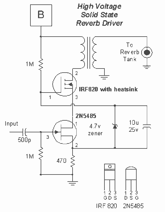
The IRF820 MOSFET has a voltage rating of 500V; it should work well in preamp stages of most tube amps. The 100-ohm resistor is there to suppress H.F. oscillations. If the IRF820 is physically close to the 12AX7 plate,...
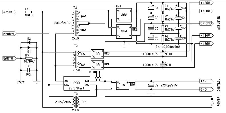
Power supply for a 1500-watt audio power amplifier. This power supply circuit is paired with a high-power audio amplifier rated at 1500 watts. A serious approach is required to design the power supply for the amplifier. First, a step-down...
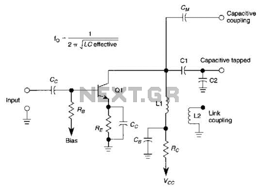
This basic tuned LC amplifier can be used with three output coupling methods: capacitive coupling output, capacitive tapped output, or link-coupled output. The tuned LC amplifier is a fundamental circuit used in various applications, including radio frequency (RF) amplification and...
.gif)
This article includes a list of references, but its sources remain unclear due to insufficient inline citations. More precise citations are needed to improve this article. Valves, also known as vacuum tubes, exhibit very high input impedance (nearly infinite...