
Operation of an Armstrong Oscillator
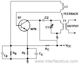
The Armstrong Oscillator operates on the principle of regenerative feedback, making it a robust choice for generating RF signals. The design includes essential components such as inductors, capacitors, and resistors, each playing a critical role in the oscillator's functionality. The tickler coil (L1) is vital for providing the necessary feedback to maintain oscillations, while the variable capacitor (C1) allows for fine-tuning of the output frequency. The choice of NPN transistor impacts the overall performance, especially in high-frequency applications. Proper biasing through resistors (Rc, Rb, Re) ensures that the transistor operates efficiently within its active region, enabling effective amplification of the oscillation signal. The configuration of the circuit—whether series-fed or shunt-fed—determines how DC and AC voltages interact within the oscillator, influencing the overall performance and stability of the output signal. The careful selection and arrangement of these components are crucial for achieving desired oscillation characteristics, making the Armstrong Oscillator a fundamental design in RF applications.An Armstrong Oscillator is a type of oscillator that uses a tickler coil which provides feedback from tank circuit. The Armstrong Oscillator is used to produce a sine-wave output of constant amplitude and of fairly constant frequency within the rf range.
Inductor L1 operates as a tickler coil, providing feedback from the output circuit [collector] to the input circuit [base] of the transistor. Inductor L1 is coupled to transformer T1, by mutual inductive coupling. between the tickler and LC tuned circuit. For the circuit to oscillator, the feedback is regenerative. The transistor is identified as a NPN transistor, and could be almost any NPN transistor. The circuit is a basic common emitter configuration. The exact transistor part number would depend on the frequency of operation of the oscillator, and the value of the voltage used as Vcc. The important criteria is that the transistor provides amplification in the frequency range of oscillation.
A 2N2222 NPN Transistor offers operation up to 300MHz. Resistor Rc is used to bias the collector of the transistor, a small loss is incurred over inductor L1, applying Vcc to the collector circuit. Resistor Rb is the base bias resistor. Resistor Re is the emitter bias resistor, also called self-bias. The capacitors Cb and Ce are used to by-pass the bias resistors for non-DC voltages. The resistors only set the DC bias, for AC voltages the resistors are shunted out of the circuit. The circuit to the right shows a series-fed armstrong oscillator. The tank circuit is form by variable capacitor C1 and the primary of T1. DC voltage is applied to the tank circuit, making the circuit a series-fed oscillator. Vcc is applied to the bottom side of the tuned circuit and is returned via T1, the collector of Q1 and emitter resistor Re [than back to Vcc].
The tank circuit is the frequency determining component of the oscillator. The frequency of oscillation is determined by the resonant frequency [Fr] which is 1 / (2 x 2. 1415927 x [LC]1/2). Trimmer capacitor C1 provides adjustments to the frequency by varying the capacitance in the tuned circuit. See Trimmer Capacitors Styles, The shunt-fed armstrong oscillator [shown in the lower side-bar] differs slightly, in that the DC voltage is no longer applied to the tank circuit.
Vcc is still connected to resistor RC, but bypasses the tank circuit and connected directly to the collector of the transistor. In addition, only AC flows into the tank circuit, capacitor C2 blocks any DC voltage from the tank circuit.
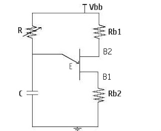
The tank circuit is now grounded to provide a return path for the output of the transistor. An oscillator that has the frequency determining components in the base of the transistor circuit, and that uses a tickler coil which provides feedback from the tuned circuit. Resistor R1 sets the amount of current through L1, the higher the adjusted value of R1 the more current flows through the L1 winding.
So the higher R1 becomes the more feedback is presented or coupled into the C1, L2 tank circuit. Trimmer R1 is adjusted so that current through L1 is sufficient to sustain oscillations in the tank circuit. In other words the resistor adjusts the gain of the feedback, the higher the resistance value the higher the amplitude of the feedback signal.
Also refer to Companies producing Trimmer Resistors. Or Common Resistor Trimmer packages in common usage. Resistor R2 sets the DC bias voltage at the base of the transistor. With power applied a small amount of base current [Vcc/R2] will flow through R2 and forward bias the base of the transistor. While the coupling capacitor C2 blocks any DC voltage from reaching the tuned circuit. Because C2 is used as a blocking capacitor, this style of circuit is a shunt-fed oscillator. The DC bias to the collector is set by the parallel combination of R1 and L1. Note that L1 is not part of the tuned circuit, so the DC current flowing through L1 does not make the
🔗 External reference
Related Circuits
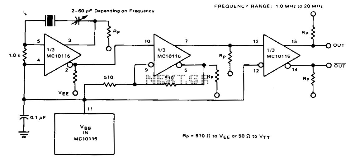
For frequencies below 20 MHz, a fundamental-frequency crystal can be utilized, eliminating the need for a resonant tank. At these lower frequencies, the typical MECL 10,000 propagation delay of 2 ns becomes negligible compared to the oscillation period, necessitating...
At the point Vp, the emitter triggers and turns the UJT (Uni-Junction Transistor) ON. Up to this point, the emitter is isolated and does not conduct, resulting in no current conduction between Base1 and Base2. The operation of the Uni-Junction...
The frequency remains stable as the voltage decreases. It is referred to as the "backwards JT" because it operates optimally with a bifilar coil and a single transistor. With a modification to the circuit, it is possible to deplete...
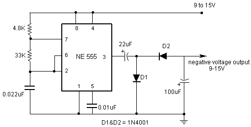
The square wave oscillator does not necessarily need to be a 555 timer; it can also be implemented using a ring oscillator with inverters. However, when utilizing 4000 series CMOS logic, the negative output voltage generated may have limited...
The chart illustrates the Wien bridge sine wave oscillator circuit. The amount of negative feedback in the circuit is determined by the internal resistance of the FET. When the peak output voltage of the oscillator reaches the regulated voltage...
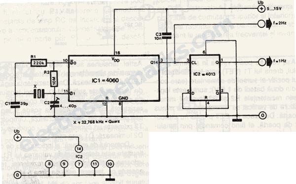
This 1 Hz and 2 Hz generator or oscillator is constructed using a 4060 IC as the oscillator and a 14-bit counter. To achieve a 1 Hz signal from the 4060, a 1/2 4013 flip-flop is utilized. This circuit...