
Output Assign Module
The output assignment module is a critical component in managing user inputs and visual feedback in electronic systems. The utilization of a 16V8 GAL for address decoding ensures efficient signal routing and reduces the complexity of the overall design. The GAL's pin configuration, as shown in Figure 44, outlines the connections necessary for proper functionality, facilitating seamless integration with the microcontroller.
For switch detection, the implementation of simple latches allows the microcontroller to efficiently monitor the status of 18 pushbutton switches. By latching the status of eight switches at a time, the design minimizes the number of components while optimizing CPU performance. Firmware debouncing routines enhance the reliability of switch inputs without the need for additional hardware, thus streamlining the circuit design. The architecture depicted in Figure 45 showcases the arrangement of these circuits, emphasizing the modularity and scalability of the input handling system.
The output assignment module also incorporates LED indicators that provide visual feedback to the user. The use of 74LS373 octal latches for controlling these indicators allows for a clean and efficient current-sinking scheme, as represented in Figure 46. This design choice parallels the fader module, ensuring consistency across the control board.
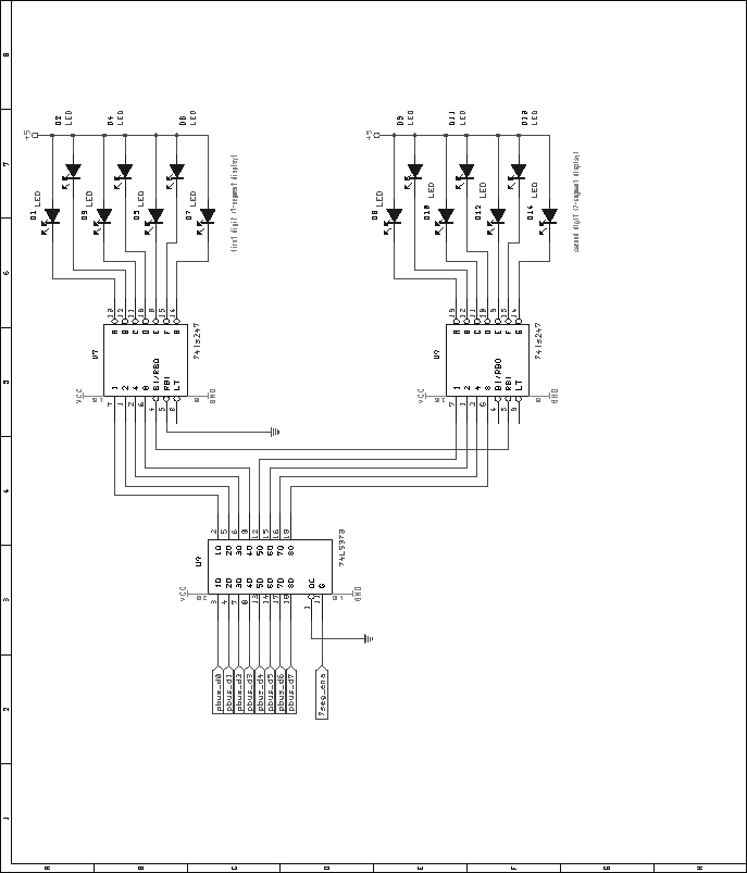
Furthermore, the inclusion of 7-segment LED displays enhances the user interface by providing clear numerical readouts. The decision to utilize BCD-to-7-segment decoders, driven by a 74LS373 latch, reflects a thoughtful consideration of bus port limitations while maintaining display functionality. The circuit illustrated in Figure 47 demonstrates the effective use of the ripple zero-blanking feature of the 74LS247 chips, which optimizes display readability by eliminating unnecessary visual clutter when displaying zero values.
Overall, the output assignment module exemplifies a well-engineered solution for managing user inputs and outputs in electronic systems, combining efficient design principles with practical implementation strategies.The output assign modules uses a 16V8 GAL for address decoding and enable signal generation. Figure 44 shows the pin assignments for the GAL used in the output assign module. The VHDL code used to generate the GALs is included in the appendices, on page The status of 18 pushbutton switches need to be sensed by the microcontroller. Many methods exi st for connecting switches to a microcontroller bus. To keep parts count and CPU use down, simple latches are used to latch the status of eight switches at a time. Firmware debouncing routines shall take the place of hardware debouncing techniques. The lack of a multiplexing scheme means less CPU time is wasted in reading in the values of the switches, while the firmware debouncing routines mean fewer components are used on the board.
Figure 45 shows the circuit used to achieve these goals. Three of these circuits are present, providing a total of 24 pushbutton inputs. Six of these inputs are used for pushbuttons in the universal user interface and cue stack sections of the control board. Figure 45: Output assign module, momentary pushbutton decoding schematic. The output assign module uses three of these circuits, for a total decoding capability of 18 on-board and 6 off-board buttons.
The output assign module contains several LED indicators that need to be controlled by the microcontroller. A simple current-sinking scheme involving 74LS373 octal latches is used, identical to that of the fader module.
Figure 46 shows the circuit. The output assign module contains a pair of 7-segment LED displays, controlled by the microcontroller. While it certainly would have been possible to drive the displays in a similar fashion to the bare LEDs present on the same board, this was decided against due to the extra bus ports needed.
Instead, BCD-to-7-segment decoders were used, with their inputs driven from a 74LS373 latch. Figure 47 shows the circuit used to drive the 7-segment displays. Note the use of the ripple zero-blanking feature of the 74LS247 BCD-to-7-segment chips. This feature will blank both displays when the a double-zero is displayed, and blank the leftmost display when its value is zero. 🔗 External reference
Related Circuits
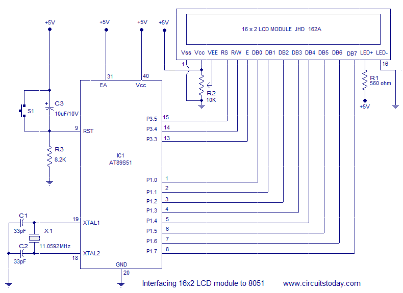
Interfacing a 16x2 alphanumeric LCD module with the AT89S51 microcontroller. The circuit diagram, theory, and program are included. JHD162 LCD module pinout and commands are provided. The integration of a 16x2 alphanumeric LCD module with the AT89S51 microcontroller involves several...
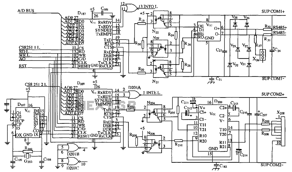
As shown in the figure, D187 is a universal asynchronous receiver-transmitter (UART). Its RX/TX signals are received through optocouplers N21, N22, and N29, facilitating RS-485 communication. The interface receiver/transmitter D28 and microprocessor D211 are completely optically isolated. D197 serves...
Have you ever wanted to create a line-following robot but found infrared sensors too expensive? If you are located in the UK and have access to a Maplin store nearby, you can purchase infrared transmitters and receivers for just...
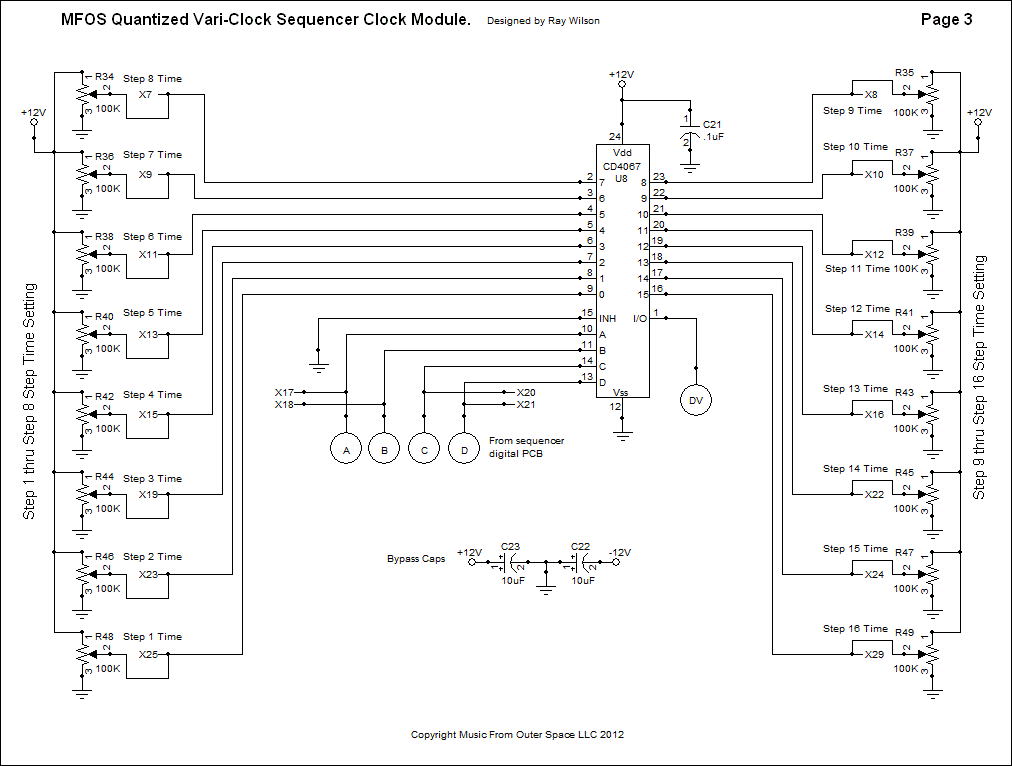
A mechanism allows a standard potentiometer to function as a digitized potentiometer, converting each setting into a number between 0 and 15. This information is utilized to determine the duration for each step. An analog-to-digital converter (ADC) is designed...
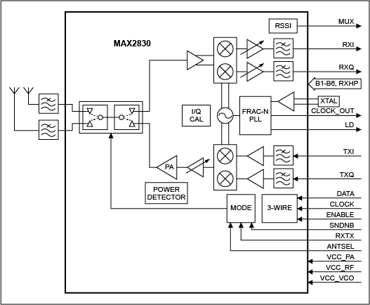
This module utilizes the highly integrated MAX2830 RF transceiver, providing a complete RF front-end solution that complies with the WLAN IEEE 802.11b/g standard. The MAX2830 RF transceiver is designed for wireless communication applications, specifically targeting WLAN systems. It integrates various...
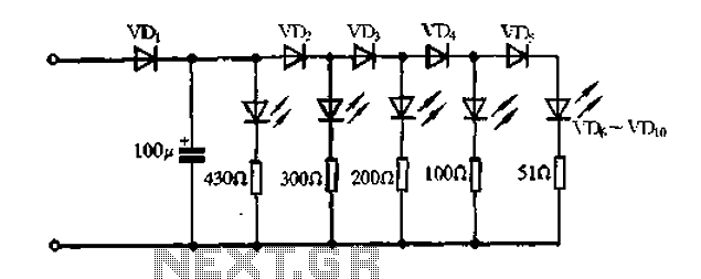
A passive light-emitting diode output level indication circuit. This circuit utilizes a light-emitting diode (LED) to provide a visual indication of the output level from a given source. The design is characterized by its passive nature, meaning it does not...