
Overtone crystal oscillator
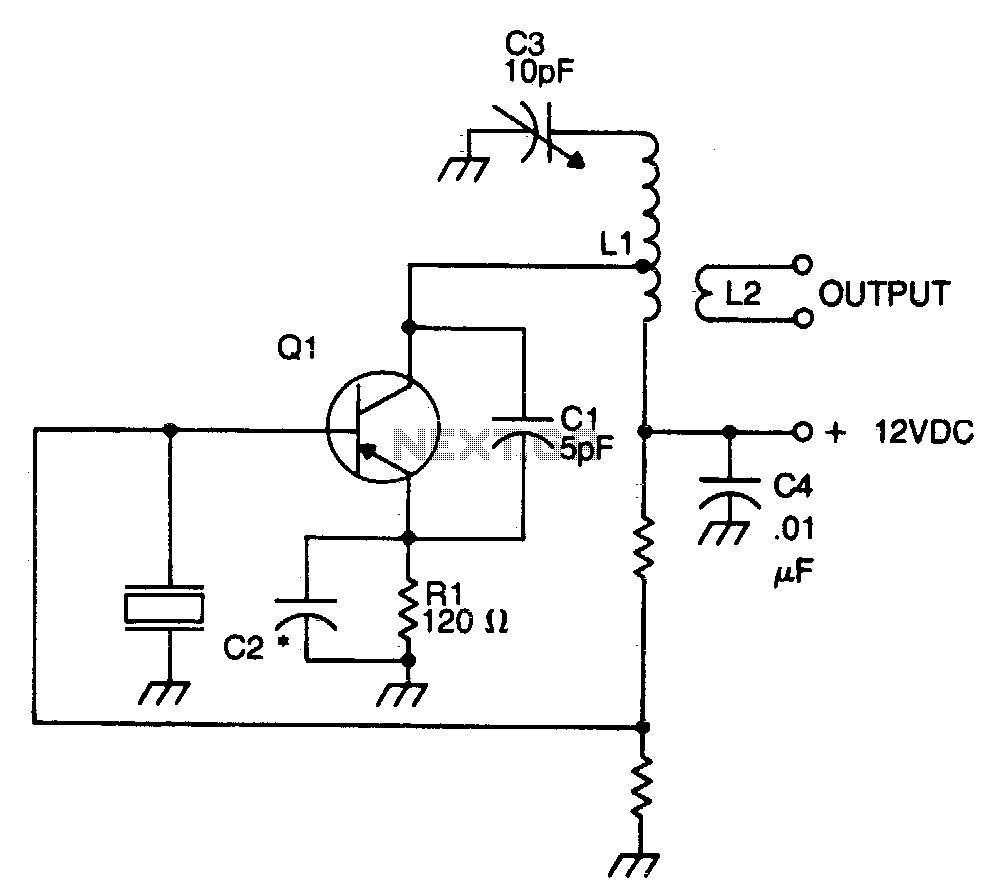
The circuit utilizes a crystal oscillator configuration, where the crystal serves as a frequency-determining element, establishing stable oscillation at its resonant frequency. The connection of the crystal between the base and ground provides a negative feedback mechanism essential for maintaining oscillation. Capacitor C1 is crucial for improving the feedback loop, compensating for the inherent capacitances present in the transistor, which can affect oscillation stability and performance. Its placement is critical; positioning it close to the transistor minimizes parasitic inductance and capacitance, thereby enhancing circuit performance.
The LC tank circuit, consisting of an inductor and capacitor, is designed to resonate at the overtone frequency of the crystal, ensuring that the oscillator operates efficiently at the desired frequency. The emitter resistor capacitor combination is designed to present a specific capacitive reactance, approximately 90 ohms, at the intended operating frequency. This value is essential for optimal performance, as it influences the gain and stability of the oscillator.
Inductor L1 features a tap that serves to match the load impedance at the collector of the transistor. This tap's placement is a critical design consideration, typically positioned about one-third from the cold end of the coil. This location is a strategic compromise, balancing the need for stability against the desire for maximum power output. The output signal is derived from the link coupling coil, L2, which operates based on transformer principles, allowing for efficient signal transfer from the oscillator circuit to the load while preserving the integrity of the signal waveform.The crystal element in this circuit is connected directly between the base and ground. Capacitor Cl is used to improve the feedback due to the internal capacitances of the transistor. This capacitor should be mounted as close as possible to the case of the transistor. The LC tank circuit in the collector of the transistor is tuned to the overtone frequency of the crystal. The emitter resistor capacitor must have a capacitive reactance of approximately 90 ohms at the frequency of operation.
The tap on inductor Ll is used to match the impedance of the collector of the transistor In most cases, the optimum placement of this tap is approximately one-third from the cold end of the coil. The placement of this tap is a trade-off between stability and maximum power output. The output signal is taken from a link coupling coil, L2, and operates by transformer action. 🔗 External reference
Related Circuits
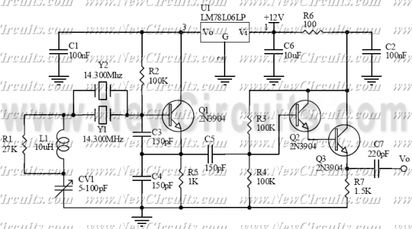
The circuit is a VXO with buffered output. It operates on the 20-meter amateur radio band with the output voltage about 0.2 Vp-p. The crystal frequency is pulled by tuning the variable capacitor CV1 about 36 kHz with only...

A circuit utilizing one 7400 TTL can operate with fundamental type crystals ranging from 1 to approximately 13 MHz. The output is rich in harmonics, making this oscillator suitable for calibration and testing applications. The circuit in question employs a...
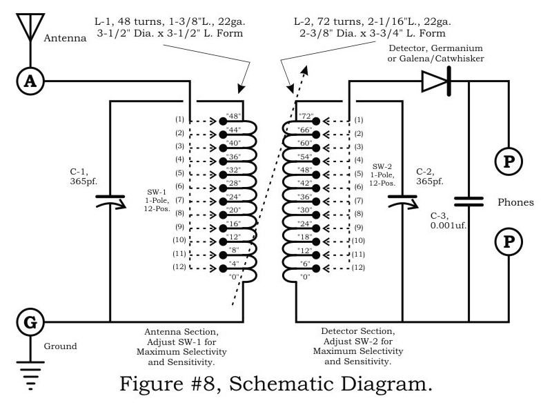
A two-circuit tuner, similar to a loose coupler, is an effective method for achieving selectivity without compromising sensitivity. The circuit introduces the signal to the primary antenna section via the SW-1 arrangement, allowing the antenna to be matched to...

Adjusting the 100 K ohm potentiometer modifies the discharge rate of capacitor Ct, thereby affecting the output frequency. A square wave output is produced. The maximum frequency achievable with CMOS technology is constrained to 2 MHz. The circuit described involves...
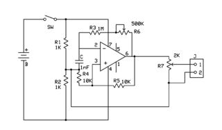
The circuit was designed to generate an oscillator that operates at low frequencies, intended for use in electronic music production, experimentation, and testing. The low-frequency oscillator (LFO) circuit typically consists of several key components, including resistors, capacitors, and an operational...
An attempt has been made to follow an instructable for some time; however, understanding its schematic remains challenging. The issue is not a lack of knowledge regarding the symbols used. In electronic schematics, symbols represent various components and their connections...