
Peak Detector

The circuit utilizes an LM392 comparator, which is a dual comparator with high input impedance and low output impedance, making it suitable for applications requiring voltage comparisons. The design begins with a 0-to-5 V input signal that is applied to the negative input of the LM392. The reset functionality is controlled by pin 12 of the DC4060BE, a binary counter IC. When this pin is pulled high and subsequently low, it resets the counter and forces the outputs of the integrated circuit ICF1 to a low state. This action results in the positive input of the LM392 also being driven low, which is critical for initiating the counting process.
With Q1 turned off, the clock oscillator of IC1, which operates at approximately 775 Hz, begins its counting sequence. The outputs from Q4 to Q14 of the binary counter are configured in a ladder arrangement, which allows for a gradual increase in voltage corresponding to the count value. As the counter progresses, it continues to increment until the voltage at pin 3 of the LM392 matches the peak voltage of the input signal. At this point, the counting process is halted, effectively capturing the peak voltage.
The output voltage, which represents the peak input voltage, is available at pin 7 of the LM392, configured as a voltage follower. This configuration ensures that the output voltage is buffered, providing a stable output that can be used in further processing or monitoring applications. The circuit's design allows for a maximum peak acquisition time of 22 seconds, indicating a relatively slow response time that is appropriate for battery-charging applications where gradual voltage changes are expected and rapid response is not critical.
Overall, this circuit exemplifies a simple yet effective method for peak voltage detection and is well-suited for applications where monitoring of input voltage levels is necessary over extended periods. A 0-to-5 V input drives the negative input of LM392 comparator if reset (pin 12) if DC4060BE is pulled high then low, all out puts of ICF1 are forced low, forcing + input of comparator to go low. Q1 is cut off and ICl"s clock oscillator, running at about 775 Hz, starts counting. The Q4 through Q14 outputs connect to a ladder. When the counter reaches a count so that the voltage on pin 3 of the LM392 equals the peak input voltage, the counter stops. This voltage is available at the output of the voltage follower LM392 (pin 7). The maximum time to acquire a peak is 22 seconds. This circuit is slow and was originally intended for battery-charging applications.
Related Circuits
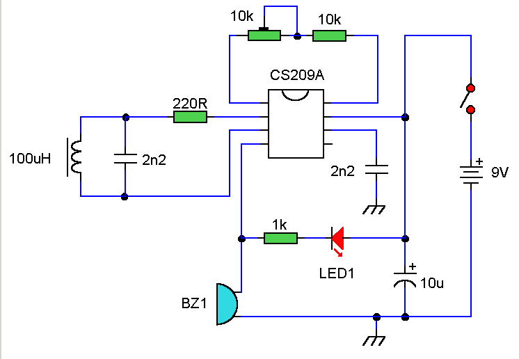
The core component of this DIY metal detector circuit is the CS209A integrated circuit (IC). The metal detector is constructed using a single 100µH coil, which has a diameter of 40 mm. The CS209A IC serves as the primary signal...
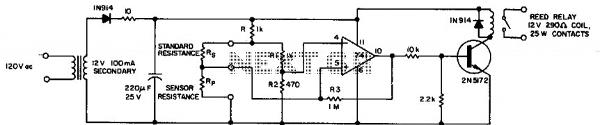
Applications such as photoelectric control, temperature detection, and moisture sensing require a circuit that can accurately detect a given resistance ratio. A simple technique that uses an operational amplifier as a sensing element can provide 0.5% accuracy with low...
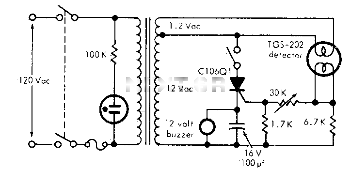
This circuit is capable of detecting smoke and various gases, including carbon monoxide (CO), carbon dioxide (CO2), methane, and coal gas, with a sensitivity of 10 parts per million (ppm). It employs a heated surface semiconductor sensor, which detects...
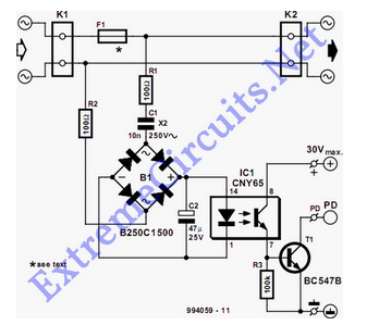
The detector is designed to sense and signal to another circuit when an appliance is connected to the mains voltage. For this purpose, an optocoupler, IC1, is utilized. The circuit employs an optocoupler (IC1) to provide electrical isolation between the...

The gas detector designed in this instance utilizes an ARM microprocessor as its core for measurement and control. It not only incorporates advanced one-chip computer microprocessing technology from the 1990s but also features several enhancements. The device employs an...
This circuit was designed to detect when a call is incoming in a cellular phone (even when the calling tone of the device is switched-off) by means of a flashing LED. The device must be placed a few centimeters...