
Phone camera flash control circuit
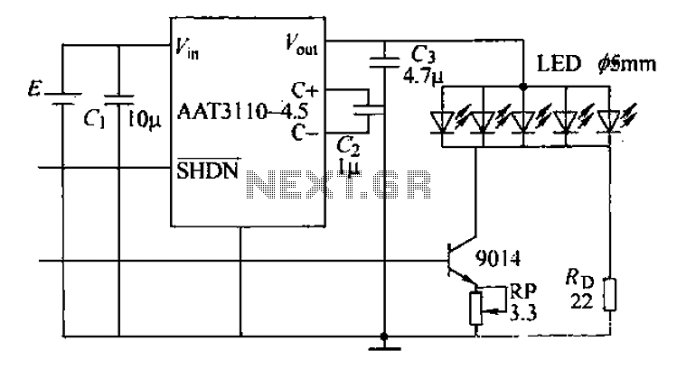
The circuit operates on the principle of a capacitive charge pump, which is a type of DC-DC converter that steps up the input voltage to a higher output voltage using capacitors as energy storage elements. The AAT3110-4.5 chip is specifically designed for such applications, providing efficient voltage boosting while maintaining a compact design suitable for mobile devices.
In this application, the lithium battery, typically around 3.7V, is boosted to 4.5V, which is suitable for driving high-brightness LEDs. The output filter capacitor (4.7µF) smooths the output voltage, ensuring stable operation of the LEDs during the flash event. The storage capacitor (1µF) temporarily holds charge to provide the necessary current during the peak flash period.
Resistor R1 is crucial for balancing the current across multiple LEDs, ensuring uniform brightness and preventing any single LED from being overdriven, which could lead to premature failure. The peak current regulation resistor RP allows for fine-tuning of the flash intensity. By adjusting the resistance value of RP, the user can control the peak current flowing through the LEDs, thus adjusting the brightness of the flash according to specific requirements.
Overall, this circuit design is optimized for providing a reliable and adjustable flash for mobile phone cameras, enhancing low-light photography capabilities while ensuring efficient power management from the device's battery.200mA peak current letter phone photo camera flash circuit, using a AAT3110-4.5 electrical capacitive charge pump chip, the phone lithium battery voltage boost and regulated to 4.5V, to a group of light-emitting diode (LED) provide work for the voltage and 100 ~ 200mA peak current. The peak current through the switch as a flash of VF form a loop. The charge pump input filter capacitor capacitance of lOtiF, output filter capacitor electric capacity 4.
7vF, storage capacitor capacitance of ltiF. Ri, LED light-emitting tube balancing resistor. RP is the peak current regulation section resistance, adjust the resistance of RP can be set peak current size.
Related Circuits

A simple USB LED lamp circuit utilizing a 5-volt power supply sourced from a USB port, designed to illuminate a desktop or laptop computer during power outages. The USB LED lamp circuit operates by converting the 5-volt DC power provided...
The metal detector consists of a probe oscillator, a reference oscillator, an audio amplifier, and various other components, as illustrated in the schematic. The probe oscillator is made up of transistors V1 and V2, a detection coil L1, a...

This device offers numerous implementation possibilities due to its wide input voltage range and large maximum output current across a broad output voltage spectrum. It features long battery life and low power consumption owing to its high efficiency and...
This simple-to-construct water fishing thermometer circuit is intended for use in sports applications, such as fishing contests. A sensor measures... This water fishing thermometer circuit is designed to provide accurate temperature readings of water, making it an essential tool for...
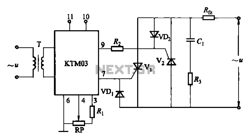
Adjustment potentiometer RP can modify the conduction angle of thyristor Vl, vz, thus altering the voltage applied across the load Rfz. The adjustment potentiometer (RP) serves a critical role in controlling the conduction angle of the thyristors Vl and vz within...

This is a VU meter analog circuit. The circuit is connected to the line terminals of the amplifier. The VU meter operates simply, with T1 and T2 indicating signal increases. The VU meter circuit is designed to visually represent audio...
Warning: include(partials/cookie-banner.php): Failed to open stream: Permission denied in /var/www/html/nextgr/view-circuit.php on line 713
Warning: include(): Failed opening 'partials/cookie-banner.php' for inclusion (include_path='.:/usr/share/php') in /var/www/html/nextgr/view-circuit.php on line 713