
Phone ringer Schematic

The described circuit is an electronic sound generator primarily utilizing oscillators and a piezoelectric transducer to produce auditory signals. The first building block is an inverter that creates a low-frequency oscillator with a timing capacitor of 1 microfarad (uF) and a resistor combination of 1 megaohm (MΩ) and 2 megaohms (MΩ). This oscillator determines the ON and OFF durations, generating a square wave signal that allows the piezo to emit sound when the output is LOW and remain silent when HIGH. The output frequency is designed to ensure that the duration of the sound and silence is equal.
The second oscillator operates at a frequency approximately double that of the first, achieved by selecting different resistor values while maintaining the same capacitance. This oscillator is responsible for producing two HIGH signals during its activation period, contributing to the overall sound output.
The third oscillator generates a frequency of 33 Hz, which simulates a bell-like ringing sound, while the fourth oscillator produces a 1 kHz tone that drives the piezo. The output from the fourth oscillator is fed into a buffer transistor, which amplifies the signal before driving one side of the piezo. The other side of the piezo is connected to the outputs of two parallel buffers, ensuring adequate pull-down capability during operation.
A notable design consideration is the insufficient drive to the left side of the piezo. Ideally, additional driving buffers would enhance the output swing, maximizing the sound produced. However, the current configuration provides a voltage swing nearly equivalent to twice the rail voltage, optimizing the sound output to a significant extent.
To provide a visual indication of the circuit's operation, the tone is also routed to an LED through a transistor. A 47-ohm resistor is employed in series with the LED to limit current flow, essential for preventing damage due to excessive current. The combined voltage drops across the LED and transistor necessitate this resistor to ensure proper functioning without pulling down the power rails.
The circuit utilizes a 1 uF electrolytic capacitor across the power rails to minimize battery impedance and maintain stable voltage levels throughout operation. A single lithium battery supplies 3V, sufficient for powering the circuit components.
Soldering considerations are paramount in this design, as excessive heat can compromise component integrity. Careful attention to soldering times and component orientation is critical to ensure reliable performance. The circuit's design emphasizes the importance of managing thermal conditions, particularly for semiconductors and other sensitive components, to avoid performance degradation or failure. Proper handling techniques during assembly are essential to maintain the operational reliability of the circuit.The circuit consists of 6 building blocks and the first is the inverter between pins 1 and 2. This forms a low frequency oscillator with a 1u and 1M + 2M2 resistor. It governs the overall timing of the ring by creating an ON and OFF time. When the output is LOW, the tone is emitted from the piezo. When the output is HIGH, the tone is inhibited and this produces the silence between the rings. This oscillator has an equal mark-space ratio to give the "rings" the same length of time as the silence. The second oscillator operates at about twice the frequency of the first (this can be seen by the different value of the resistors as both capacitors have the same value).
The frequency has been adjusted so that it produces two highs during the interval when it is activated. The second oscillator does not produce two full cycles but only one and a half as it is the HIGHs that are required.
During each of these HIGHs, the third and fourth oscillators produce a warble that simulates the 33Hz ring of the "bell." The third oscillator generates the 33Hz frequency and this gates the fourth oscillator to produce a 1kHz tone for the piezo. The output of this oscillator drives the base of the buffer transistor and also one side of the piezo.
The other side of the piezo is connected to the output of two buffers in parallel and this provides good pull-down capability when the left side of the piezo is high. The only fault in the design of this circuit is the drive to the left-hand side of the piezo. We should have included driving buffers to give it the maximum swing and thus the maximum output. But since we did not have any left over, this is the best we could do. When the piezo is driven from a pair of buffers on each side, it sees a voltage swing of nearly twice the rail voltage and this gives it the highest output.
The tone is also passed to a LED via a transistor to give a visual indication of the operation of the circuit. A 47R resistor has been included in series with the LED to limit the current. It is essential to include a resistor as the LED drops a fixed voltage (called the characteristic voltage drop) when it is illuminated and the transistor drops a fixed voltage across the collector-emitter terminals when it is turned on.
The voltage drops are 1 .7v for the LED and .5v for the transistor. This adds up to 2.3v and thus we must include a resistor to drop .7v from the 3v supply rail. By making the resistor 47R we allow a maximum of 1.4mA to flow. Without this resistor the power rails would be pulled down to 2.3v every time the LED is turned on. This would cause (a) a very high current to flow through the LED and (b) faulty operation of the circuit as the power rails fluctuate. The 1u electrolytic across the power rails reduces the impedance of the battery and provides uniform rail impedance during the life of the battery.
A lithium battery has been used as it produces 3v so that we only need a single cell to provide the minimum voltage for the chip. Don't press too hard with the clip or the iron and don't move the component with the iron as this will make it stick to the tip and cause it to heat up too much.
When you have soldered one end, wait a few seconds before soldering the other as this will allow the component to cool and prevent it getting too hot. This is important as the temperature of the tip of the iron will be about the absolute maximum any of the components can tolerate and the only way to prevent damage is to limit the soldering time to one or two seconds.
The reason for this is the junctions of the semiconductors are very close to where the soldering is taking place and any overheating will cause degeneration in performance and even premature failure. The LEDs are also very critical as the light-emitting crystal will lose its output at the slightest amount of overheating.
The transistor will lose gain if overheated while the signal diodes are slightly more tolerant however they become leaky if subjected to too much heat. The electrolytics can also suffer considerably by overheating, so take care. While taking care with the temperature and soldering times, you must also remember the orientation of the components as they will not work if placed around the wrong way.
The placement of the transistor is fairly obvious as it has three leads and you can see which way around it goes. The diodes come in the same package as the transistor and you must not confuse the two. 🔗 External reference
Related Circuits
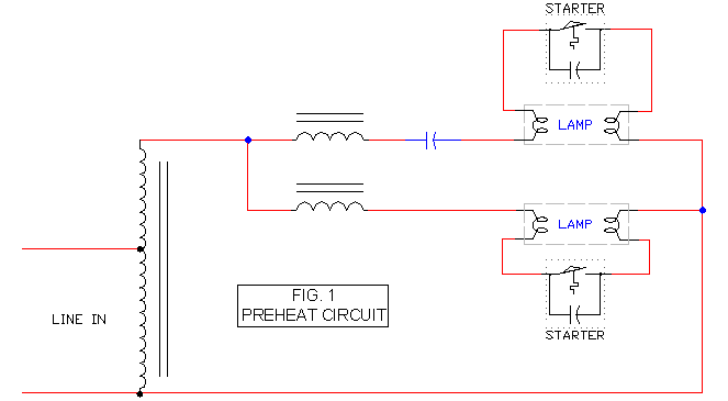
It includes a starter for each lamp that heats the filaments (cathodes) at both ends of the lamp before ignition. Once the lamp is lit, the heated filaments are no longer necessary. The heating serves solely as an ignition...
The circuit consists of two main components: (1) a power supply circuit featuring a transformer (T) that steps down AC 220V to 33V, followed by a full-wave rectifier, a filter, and a three-terminal regulator that outputs +24V. This circuit...

Approximately 20 years ago, small key-holders that emitted an intermittent beep for a few seconds upon detecting a whistle were quite common. These devices utilized a specialized integrated circuit (IC) that made them unsuitable for home construction. The current...
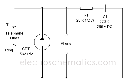
This circuit provides protection for telephones, EPABX systems, telephone modems, and similar devices against lightning discharges and line voltage spikes. It incorporates a safety capacitor and gas discharge components. The circuit employs a safety capacitor to filter out high-frequency noise...

Working on Strowger phone exchanges involves a significant amount of soldering. However, unlike modern electronics, it is not possible to use a temperature-controlled soldering station with a built-in solder stand when working up a ladder. Typically, only a 50V...
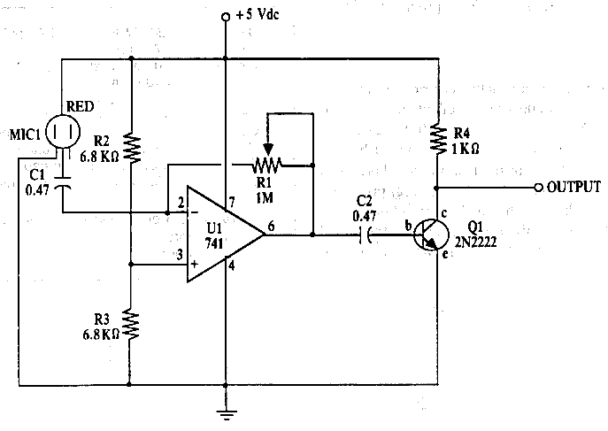
Amplifier circuit for electret microphones (condenser microphones). It amplifies the audio signals picked up by the electret microphone using a 741 op-amp and a 2N2222 transistor. The amplifier circuit designed for electret microphones utilizes a combination of a 741 operational...