
pic based wwvb clock

The WWVB clock design is a robust system that relies on the precise timing of the WWVB signal. The 60 kHz carrier frequency is ideal for long-range transmission, enabling the clock to receive time signals from considerable distances. The clock's microcontroller, the PIC 16F628, is well-suited for this application due to its low power consumption and sufficient processing capabilities to handle the decoding of the time code.
The choice of 7-segment displays allows for clear visibility of time, while the design cleverly utilizes decimal points to enhance the display's readability. The microcontroller's design ensures that the time is updated accurately and promptly, contributing to the overall reliability of the clock.
The implementation of a "bare-bones" PCB design not only reduces costs but also simplifies the assembly process. The decision to use an external power supply helps eliminate potential interference from internal components, ensuring a more stable operation.
Overall, this WWVB clock design exemplifies an effective integration of RF signal processing, microcontroller programming, and user-friendly display technology, making it a practical solution for accurate timekeeping applications.The WWVB signal is broadcast as a 60 kHz carrier that is AM modulated with a time code frame that is updated once per minute. The data rate is one bit per second. Along with time code information, the data frame also contains synchronization bits, calendar data, UT1 correction, leap year, and leap second data.
The clock design presented here only decodes the time data and daylight savings correction data. The software could easily be modified to include decoding of the other information bits, if desired. The the low frequency WWVB signal strength is weak and reception can be problematic. Signal acquisition time is variable, depending on location and atmospheric conditions. Reception is usually best at night between 8pm - 4am. To use the clock, just apply power and wait for reception of the WWVB signal. When the clock receives a complete error-free frame of data, it will automatically reset the display to show the correct time.
After the initial time correction, the clock will maintain time even if WWVB reception is lost. As shown in the schematic (pdf format), the heart of the clock is a PIC 16F628 microcontroller running at 4 MHz. Decoded time data is sequentially output from the microcontroller (RA0 - RA3) to the 7-segment decoder/drivers on a 4-bit data bus.
The data is output sequentially as seconds, 10s of seconds, minutes, 10s of minutes, hours, and 10s of hours. The microcontroller outputs (RB1, RB2, RB3) route a 10 uSec stroble pulse from RB4 out to each of the 7-segment decoder/drivers at the proper time to latch the data bus values.
Seconds and 10s of seconds display values are updated once per second. Minutes, 10s of minutes, hours, and 10s of hours are updated once per minute. The display consists of 1" red-orange LED 7-segment displays. The decimal points on the displays are used to form colons to separate the seconds, minutes, and hours. The 10s of seconds and 10s of minutes displays are mounted upside down to form the upper colon dots. The WWVB receiver is a C-MAX model CMMR-6 and is available from Digi-Key ( as part # 561-1014-ND complete with loopstick antenna.
Data output from the receiver is sampled by the microcontroller on RB0 I have built two of these clocks, one using point-to-point wiring and one using a pcb. Both versions perform well. Just keep the receiver away from noise sources and the wire / trace lengths short to minimize inductance.
I found that the receiver is also sensitive to magnetic fields produced by power supplies. I used a 9V, 200 mA "wall-wart" instead of an internal power supply to eliminate this problem. My pcb was designed using Free PCB software. The artwork contains both the main board and the display board on a single layout to save the cost of two separate boards. I purchased the pcb from by sending them the gerber files and using their "bare-bones" process. The "bare-bones" process does not include solder mask nor silk-screen. Just cut off the display board from the main board and mount it at a right angle to the main board and wire them together using the pads provided.
The software is interrupt driven, from the PIC Timer 2 module. The basic timing is set to provide 32 interrupts/sec for both receiver sampling and for internal time propagation. The received data is sampled at 32 samples per second. The software cross correlates the input samples with stored "ideal" samples of the one, zero, and syn
🔗 External reference
Related Circuits
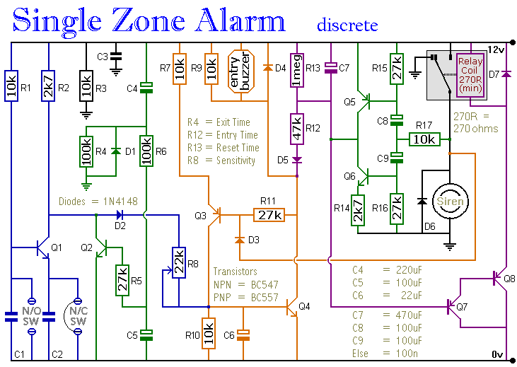
The circuit includes automatic exit and entry delays, a timed bell cut-off, and a system reset feature. It accommodates both normally-open and normally-closed switches, making it compatible with standard input devices such as pressure mats, magnetic reed contacts, foil...
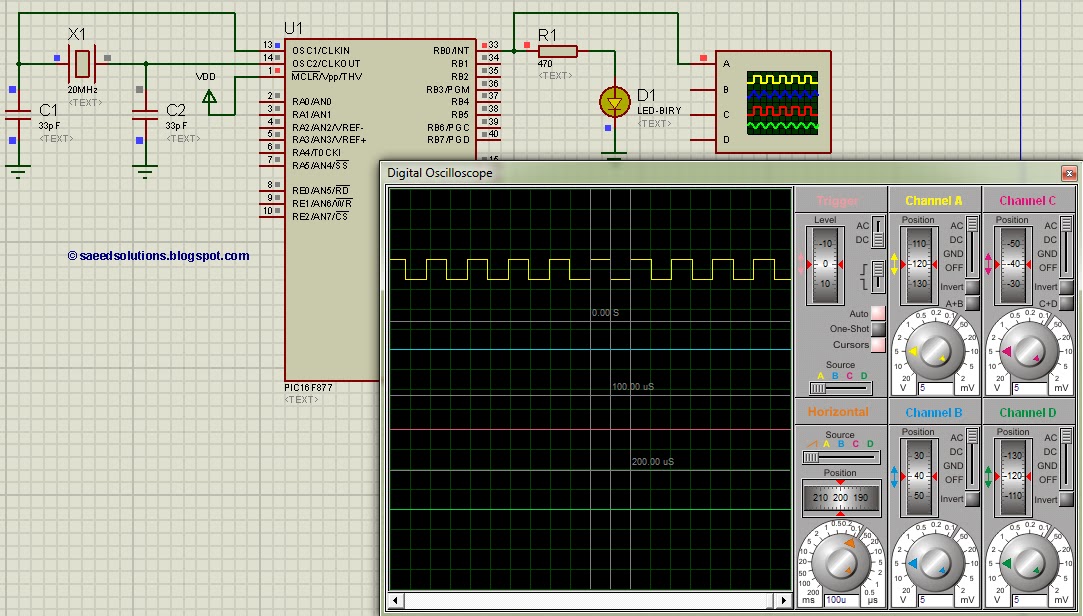
This tutorial on the PIC16F877 microcontroller addresses the question of how to utilize Timer0 and manage its interrupts. It utilizes the PIC16 simulator for demonstration purposes. The PIC16F877 microcontroller is a versatile device widely used in embedded systems. Timer0 is...
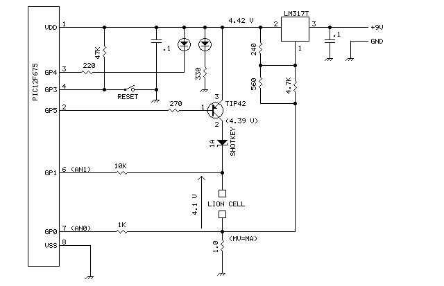
Lithium Ion batteries pack a lot of power by weight compared to other types. There are 2 things that need to be handled differently than nicad or NiMH. They cannot be used as a direct substitute (even if they...
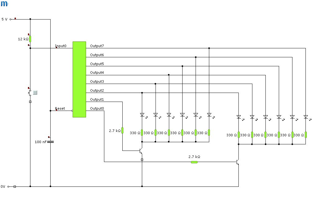
A series of digital clocks with LED outputs were developed for the Electronics in Schools Strategy (EiSS) and utilized in various courses organized by SETPOINT (now STEMPOINT) Devon & Cornwall for secondary school educators in the southwest. The initial...
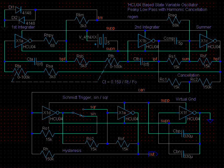
This circuit is based on the State Variable Band Pass Filter, incorporating amplitude-limited regenerative feedback. The State Variable Band Pass Filter (SVBPF) is a versatile filter design that allows for simultaneous control over the center frequency, bandwidth, and gain. This...
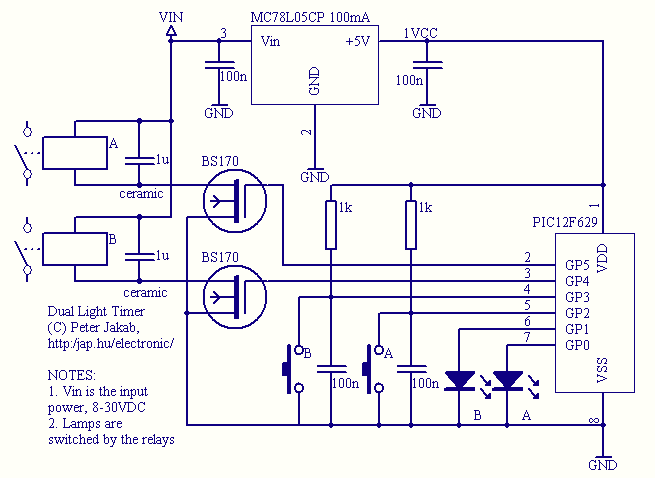
This is a lamp timer capable of operating two separate relay switches. Outputs can be in three (or restricted to two) states: OFF, delayed ON and constant ON. Delayed ON mode is indicated by the LEDs. The source code...