
PLL Stereo FM Transmitter
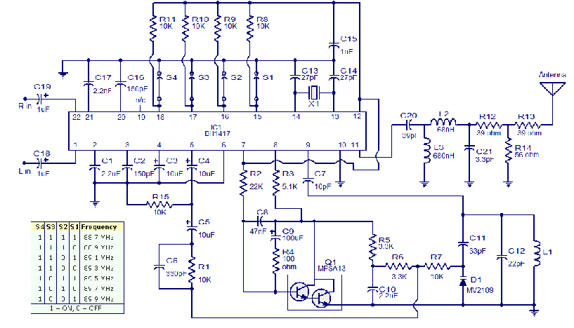
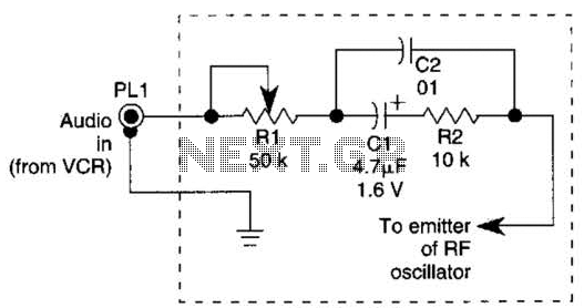
Capacitors C18 and C19 serve as DC decoupling capacitors for the left and right channel inputs. Capacitors C1 and C17 determine the pre-emphasis amount, set here to 50µS. Capacitors C2 and C16 establish the roll-off point for the low-pass filter. The crystal X1, with a frequency of 7.6 MHz, sets the oscillator frequency, with capacitors C13 and C14 providing the necessary loading. Resistors R8 to R11 act as pull-up resistors for the D0 to D3 pins (15 to 18 of the IC), which can be pulled low by closing the corresponding switches. The RF oscillator is tuned using components L1, C11, C12, and D1, where capacitor C11 prevents DC voltage from reaching the varicap diode D1, thus avoiding current flow into inductor L1. Additionally, it mitigates the effects of capacitance changes in D1 on pin 9. Capacitor C7 similarly prevents DC current from pin 9 flowing into inductor L1. The composite output signal at pin 5 is routed through a network comprising components C4, C5, C6, and R1 to the junction of resistors R6 and R7. Pin 19 of the circuit remains unconnected, although an optional capacitor can be added to set the pilot level and phase, which is not essential for circuit operation.
The composite output signal experiences attenuation as it passes through the network before reaching varicap diode D1. The carrier frequency is regulated by the PLL phase detector output pin (pin 7) and the associated components. The Darlington transistor Q1 is activated by the output from pin 7, applying a control voltage to the varicap diode through resistors R5, R6, and R7. Capacitor C10 functions as a high-frequency filter, while R7 provides isolation. Resistor R4 and capacitor C9, connected in series between the collector and base of Q1, enhance the transient response of the transistor and improve low-frequency filtering, respectively. Capacitor C8, placed between the collector and base of Q1, adds further high-frequency filtering. Resistor R3 acts as the collector load for transistor Q1. The modulated RF output is available at pin 11 and is sent to the antenna via a filter network composed of components L2, L3, C20, and C21, which eliminates harmonics. Resistors R12, R13, and R14 reduce the signal level to the antenna, thereby decreasing the transmitter's output power, a necessary adjustment to comply with legal limitations in many jurisdictions regarding transmitter output power above a few milliwatts.The circuit shown here is of a good Stereo FM transmitter that can transmit high quality signals up to a range of 70 feet. The circuit is based on BH1417 PLL stereo transmitter IC from Rhom semiconductors. The IC has separate audio processing sections for the left and right channels, pre emphasis circuit for improving signal to noise ratio, crysta
l control circuitry for accurate frequency locking, multiplex circuit for making sum ( left plus right) and difference ( left minus right) {see this article for better understanding Stereo decoder circuit} etc. Another important feature of this IC is that the transmission frequency can be set using a 4 channel DIP switch.
The IC can be powered from anything between 4 to 6V DC and has an output power around 20mW. At full output power the circuit consumes only 20mA and has a channel separation of 40dB. There are 14 possible preset transmission frequencies, starting from 88. 7MHz and incrementing in steps of 0. 2MHz that can be selected using the DIP switch. The PLL circuitry of the IC is so precise that there is practically no frequency drift. Circuit Description Capacitors C18 and C19 are DC decoupling capacitors for the left and right channel inputs. Capacitors C1 and C17 are used to set the amount of pre-emphasis required and here with the used values it is 50uS.
Capacitors C2 and C16 sets the roll-off point of the low pass filter. The crystal X1 is a 7. 6MHz crystal which sets the oscillator frequency while capacitors C13 and C14 associated with are used for providing the appropriate loading. Resistors R8 to R11 are the pull-up resistors for the D0 to D3 (pins 15 to 18 of the IC) respectively.
These pins can be held low by closing the corresponding switches. The RF oscillator of the IC is tuned using the components L1, C11, C12 and D1. Capacitor C11 prevents and DC voltage being applied to the varicap diode D1 and thereby prevents current flow into the inductor L1. More over it reduces the effects of changes in the capacitance of D1 on the pin 9. Capacitor C7 prevents any DC current from flowing into the inductor L1 from pin 9 of the IC. The composite output signal at pin 5 is applied to the junction of R6 and R7 though a network comprising of components C4, C5, C6 and R1.
In the circuit pin 19 of the circuit is left unconnected, but an optional capacitor at this pin can be used to set the pilot level and phase. Any way such a capacitor is not at all a necessity here and the circuit will work perfectly even if the capacitor at pin 9 is omitted.
The composite output signal undergoes some attenuation while passing through this network and finally reaches the varicap diode D1. The carrier frequency is controlled using the PLL (phase lock loop) phase detector output pin (pin 7) and the components connected around it.
The darlington transistor Q1 is driven by the output of the pin7 and the transistor applies a control voltage on the varicap diode through resistor R5, R6 and R7. Capacitor C10 works as a high frequency filter while R7 is meant for isolation. Resistor R4 and capacitor C9 connected in series between the collector and base of Q1 provides further filtering.
Resistor R4 improves the response of the transistor to transient changes while capacitor C9 improves low frequency filtering. Capacitor C8 connected between collector and base of Q1 provides additional high frequency filtering.
Resistor R3 serves as the collector load for the transistor Q1. The modulated RF output is available at pin 11 and it is fed to the antenna through a filter network consisting of components L2, L3, C20, and C21. The job of this filter network is to remove harmonics. Resistors R12, R13 and R14 reduces the signal level to the antenna and as a result decreases the output power of the transmitter.
Such a reduction is necessary to make the transmitter legal because in many countries transmitters that has an output power more than few milli wa 🔗 External reference
Related Circuits
This continuous wave (CW) transmitter is capable of producing an output power of up to 3 watts. By applying a 24-volt supply to transistor Q2, the output power can be increased to as much as 10 watts. It is...
This is a stereo LED level meter. It is the most affordable and effective bar graph display available, utilizing commonly accessible components. The circuit requires only a few LEDs, 22 transistors, some resistors, diodes, and a set of electrolytic...
The measured output power and efficiency of a 6 dBm 130nm CMOS class-D inverter chain was analyzed, utilizing gate bias variation to generate a pulse width modulated inverter output voltage (Cijvat et al., 2008). Efficiency versus output power was...
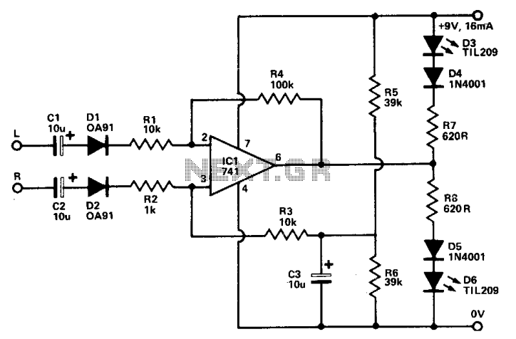
To utilize the indicator, set the amplifier to mono mode and modify the balance control until both LEDs are equally lit. The amplifier is now in optimal stereo mode balance. The circuit described involves an amplifier with a built-in indicator...
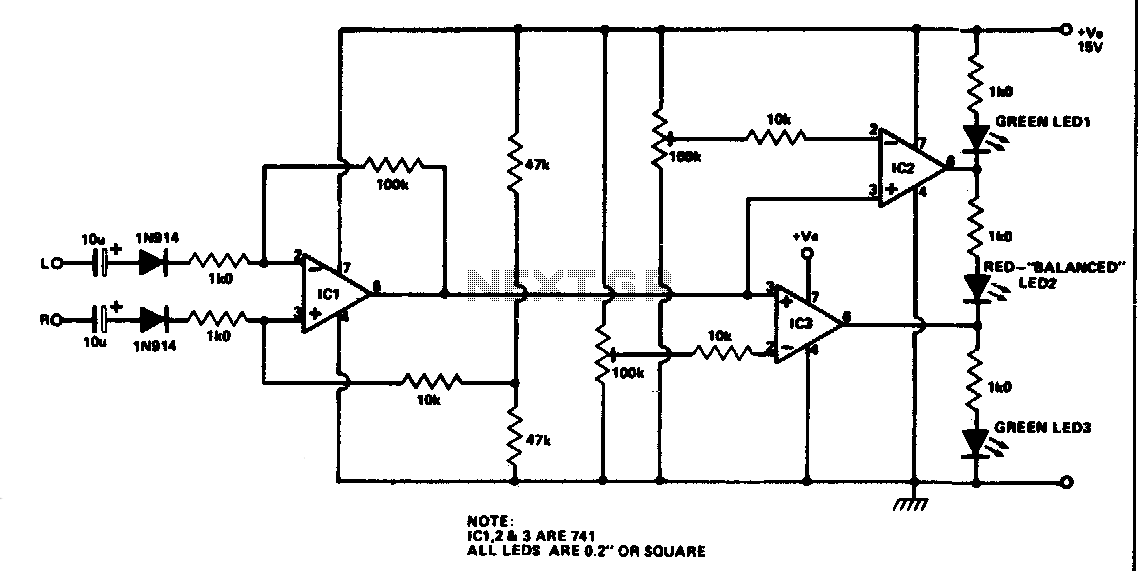
Outputs from each channel are fed to the two inputs of IC1 connected as a differential amplifier. IC2 and IC3 are driven by the output of IC1. The output of IC1 is connected to the non-inverting inputs of IC2...
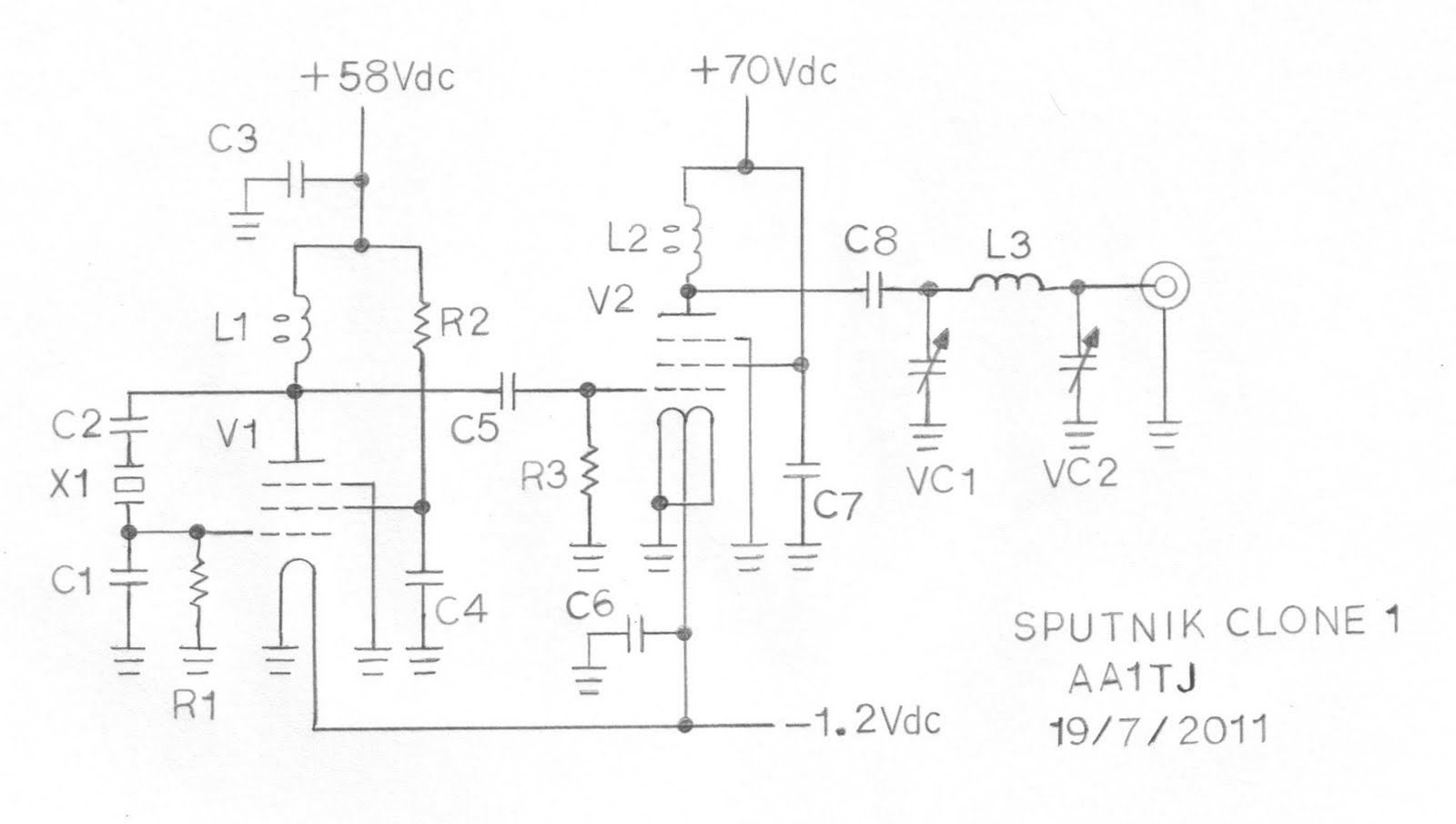
This document describes a prototype transmitter for the Sputnik QSO Party. The RF output power is 450 mW, with 70 V DC at 14.4 mA on the V2 anode. The screen current (G2) for V2 is 1.6 mA, while...
Warning: include(partials/cookie-banner.php): Failed to open stream: Permission denied in /var/www/html/nextgr/view-circuit.php on line 713
Warning: include(): Failed opening 'partials/cookie-banner.php' for inclusion (include_path='.:/usr/share/php') in /var/www/html/nextgr/view-circuit.php on line 713