
power mosfet circuit
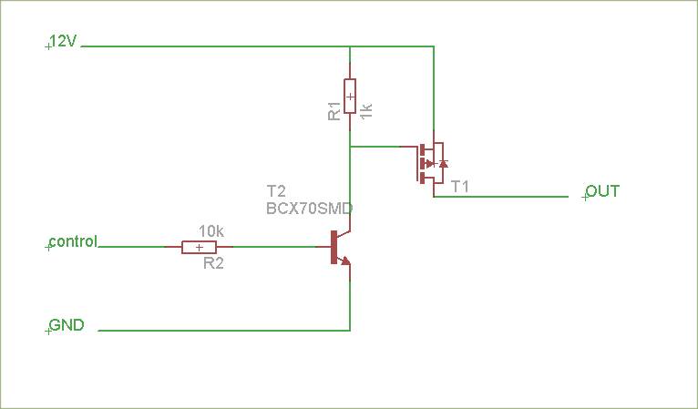
In the proposed circuit, the P-channel MOSFETs serve as the primary switching elements for controlling the output voltages. It is crucial to ensure that the gate-source voltage (Vgs) is correctly managed to achieve the desired ON and OFF states of the MOSFETs. When the gate voltage is lower than the source voltage by the threshold voltage of the MOSFET, the device will turn ON, allowing current to flow from the source to the drain. Conversely, when the gate voltage is equal to or higher than the source voltage, the MOSFET turns OFF, interrupting the current flow.
To implement reverse polarity protection, a common solution is to introduce a diode in series with the power supply. This diode will block any reverse current that could damage the MOSFETs or other components in the circuit. An alternative method is to use a P-channel MOSFET in a high-side configuration, which can also provide reverse polarity protection when correctly biased.
Given that the switching frequency is low (less than 1 kHz), the design can be simplified by removing components that are necessary for high-frequency operation. This includes reconsidering the need for a fast MOSFET driver, which may not be required for applications that do not demand rapid switching. Instead, a simpler approach could involve directly driving the gate of the P-channel MOSFET using a resistor and a pull-down configuration to ensure that the gate is pulled to ground when the control signal is low.
In summary, the circuit can be optimized by ensuring proper gate voltage management, integrating reverse polarity protection, and simplifying the driver circuitry for low-frequency applications. This approach will enhance reliability while reducing component count and complexity.The schematic is attached, I`d like to have a suggestion if any improvement could be made, in particular I`d need to add a reverse polarity connection protection. I`m not a MOSFET expert, but: from the schematic I take it that the logic level inputs (5 V) are meant to control two output voltages (12V) via P-channel MOSFETs.
1) The P-channel MOSFET s are ON (conducting) when the gate-source voltage is negative. This means that the MOSFET will be OFF when the output of the MOSFET driver is high (12 V). See datahseet of the MCP14E3, table 4-1. I don`t know whether you are aware of this and whether this is the intended behaviour. 2) The MOSFET driver circuit is meant for fast switching operation. Do you really need to switch power very fast If you are only going to switch power on and off now and then (meaning at less than e. g. 1 kHz), you can simplify the circuit tremendously: 🔗 External reference
Related Circuits
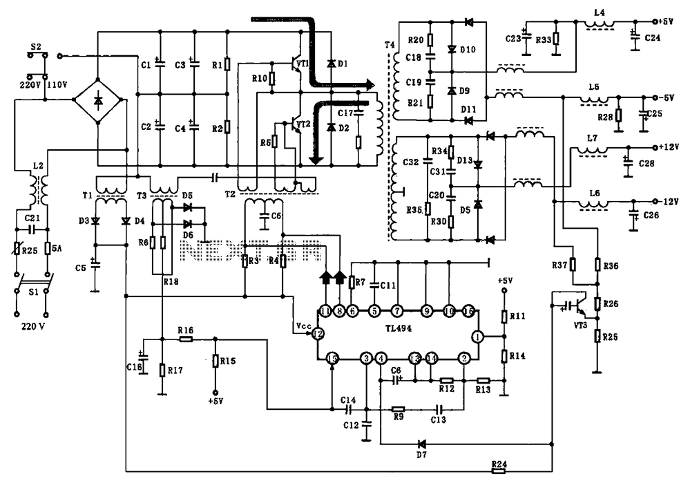
The BE-150 mainframe computer features a switching power supply circuit. The circuit utilizes the oscillation control IC TIA94. A 22V voltage is supplied through the power switch S1, fuse, filter capacitor C21, L2, and a mutual inductance filter, which...
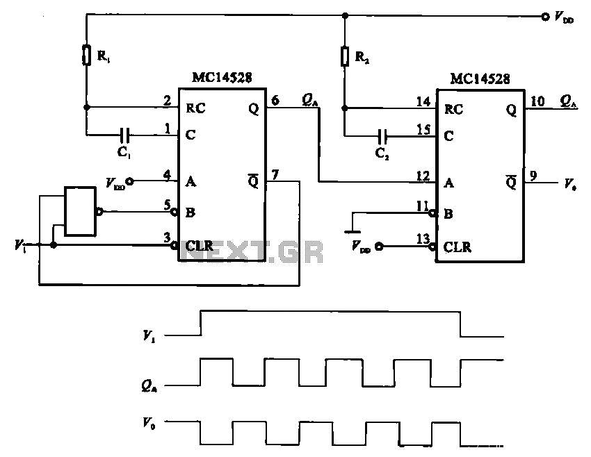
The pulse generating circuit monitors signals using monostable flip-flops. It generates a single-shot output signal based on the input pulse signal. A key signal from the monostable flip-flops is represented in a formula, with the input (V1) and output...
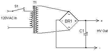
The circuit can produce about 250-500mA at 2KV, depending on the transformer. For C1, you can use the capacitor out of an old microwave. This circuit is mainly provided as a demonstration of using commonly available parts for something...
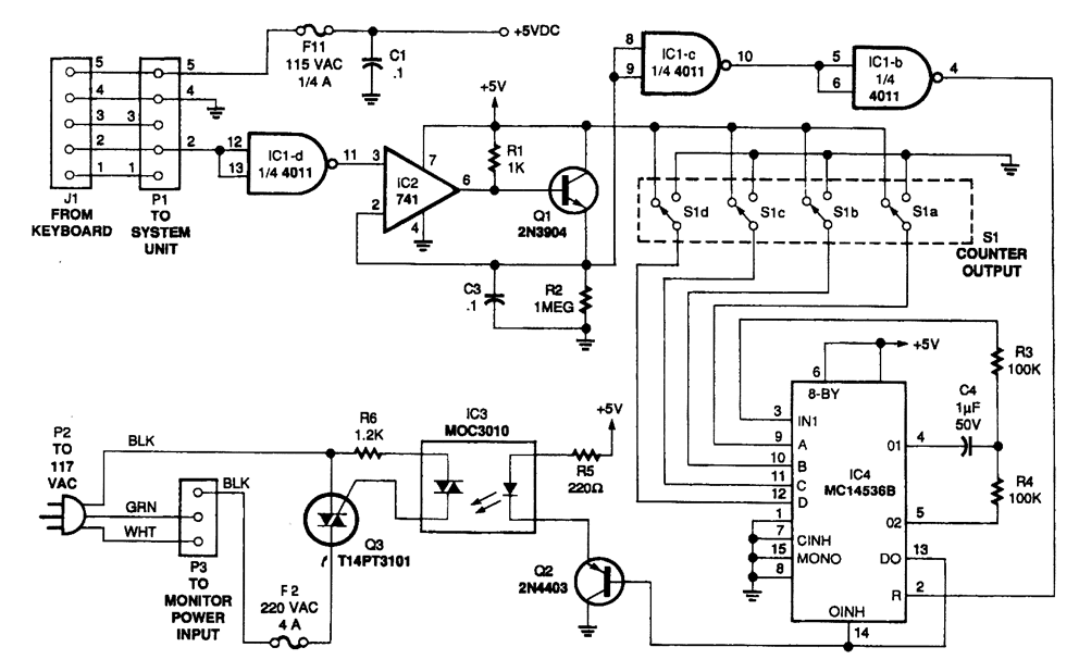
The circuit monitors PC keyboard activity through a five-pin DIN connector J1. When a key is pressed, the keyboard transmits a series of negative-going pulses on pin 2. In conjunction with Q1 and C3, the operational amplifier operates as...
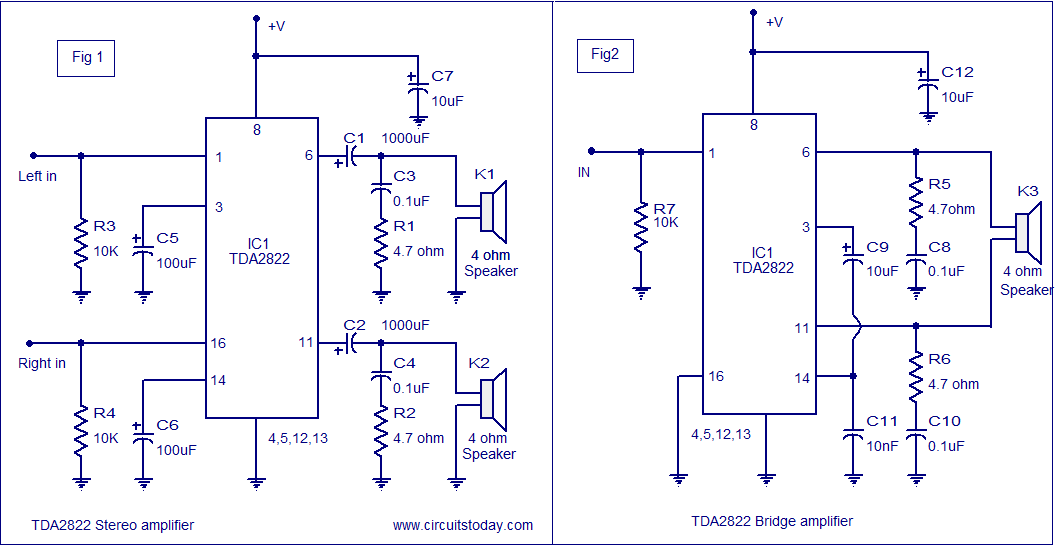
The TDA2822 audio amplifier circuit provides 1.35W output into a 4-ohm speaker when powered by a 6V supply. It supports both bridge and stereo modes and operates within a supply voltage range of 3V to 15V, making it suitable...
This circuit features a simple, highly sensitive capacitive ON/OFF switch pad that changes the state of a latch and activates an LED without requiring physical contact. The pad can be insulated, and a range of 12mm is easily achievable...
Warning: include(partials/cookie-banner.php): Failed to open stream: Permission denied in /var/www/html/nextgr/view-circuit.php on line 713
Warning: include(): Failed opening 'partials/cookie-banner.php' for inclusion (include_path='.:/usr/share/php') in /var/www/html/nextgr/view-circuit.php on line 713