
Prepping Residential Gateways for WAN Access
The design of a residential gateway with an integrated ADSL modem/router necessitates careful consideration of the WAN interface to ensure optimal performance and reliability. The AFE plays a pivotal role in this architecture, handling the critical tasks of signal conditioning and conversion. The integration of high-pass and low-pass filters is essential to maintain signal integrity by preventing interference between the ADSL and POTS signals. The use of a VCXO for clock recovery is also vital, as it synchronizes the modem with the central office, ensuring stable data transmission.
Engineers must also focus on the layout of the PCB to minimize noise coupling between components, which can significantly affect performance. The selection of components, particularly those in the Rx and Tx paths, should prioritize low noise and high linearity to maximize the effective range of the ADSL connection. Additionally, the design must accommodate various environmental factors, such as temperature variations, which can influence the performance of analog components.
In summary, the development of a residential gateway with ADSL capabilities involves a complex interplay of analog and digital technologies, requiring meticulous attention to detail in both the design and implementation phases to achieve a robust and efficient communication solution.Much of the focus around residential gateways designs has focused on distributing communication connectivity within a home or residence. But, in order to distribute content, gateways must first have an effective WAN interface that provides access to cable modem, fixed broadband wireless, or DSL broadband pipes.
In this article, we`ll explore someof the design challenges that engineers will face when building the WAN portion of a residential gateway design. Specifically, we`ll look at the challenges of building an ADSL modem/router into a gateway without jeopardizing the performance of the ADSL signals. The interface to the ADSL line is composed of a set of discrete circuits as well as an ADSL chip set.
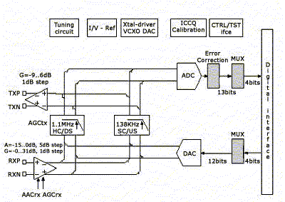
In general, the analog chip, termed the analog front end (AFE) [See Figure 1], incorporates all the analog-to-digital conversion, digital-to-analog conversion, and filtering functions required to acquire and create the characteristic discrete multi-tone (DMT) signal. For many ADSL modem designs, the receive side (Rx) of the AFE will first filter the DMT signal coming from the line to the AFE chip using a plain old telephone system (POTS) high-pass (HP) filter for attenuation of speech and POTS signaling.
This method also prevents the ADSL signal from leaking into the POTS bandwidth. A channel filter is also used for attenuation of the echo signal to improve the characteristics of the Rx path, or the maximum amount of useful amplitude allowed within the chip. The signal is amplified by a low noise gain stage (-15 to +31 dB) and is follow by a low-pass signal that is filtered to avoid anti-aliasing and to ease further digital processing by removing unwanted high-frequency, out-of-band noise.
A 13-bit analog-to-digital (ADC) converter samples the data at 8. 832 Mbps, transforms the signal into a digital representation, and sends it to the DMT signal processor via the digital interface. On the transmission side (Tx) of the AFE, the 12-bit data stream at 8. 832 Mbps coming from the DMT signal processor, through the digital interface, is transformed by a digital-to-analog converter (DAC) into an analog signal.
This signal is then filtered to decrease DMT sidelobe levels and meet the transmitter spectral response outlined in the American National Standards Institute (ANSI) specifications. This filter stage also reduces the out-of-band noise, which can be echoed to the Rx path, to an acceptable level.
The pre-driver buffers the signal for the external line driver and, for short loops, can control the level of attenuation (between -9 and +6 dB) before the signal reaches the line driver. In the United States, a band-pass filter must be used between the AFE and the line. The high-pass part of this filter (Fc=30 kHz) ensures that no ADSL signals leak in the POTS band. The low-pass filter (Fc=125 kHz) keeps the Tx signal from interfering in the Rx band and overloading the Rx stage.
The AFE often includes the circuitry to support the voltage-controlled crystal oscillator (VCXO), which acts as a slave to the clock on the central office side. The VCXO, the receive path circuitry, board layout, and component selection are the three most important factors when creating an ADSL WAN subsystem that can support long-reach performance up to 12 km.
These three factors play a dominant role in suppressing noise to ensure the best performance in the ADSL modem. Let`s first take a look at the requirements for the VCXO circuitry. The ADSL modem on the CPE extracts the clock to synchronize the central office and the CPE —basically a clock recovery scheme using a discrete VCXO.
For the VCXO function, the designer can select an off-the-shelf solution. However, as this approach is expensive, most companies construct a VCXO circuit from discrete devices for a cost-effective alternative. An important note: to ensure no noise present within the VCXO is spread, the designer can use an inductor/capacit
🔗 External reference
Related Circuits
The following alarm circuit is designed with features that may be suitable for residential and commercial alarm system applications. It has a 12V and 1.5A regulated power supply. Furthermore, this residential alarm circuit also includes a delay circuit, a...
Twang is a guitar sound that closely resembles that of a banjo or mandolin. The circuit generates distinctive sounds from a standard electric guitar by eliminating the bass frequencies, heavily distorting the midrange and treble frequencies, and subsequently amplifying...
This page presents an alternative method to directly control the stepper motor board of your mount. The functionality for controlling the stepper motors remains largely unchanged from the original modification, as both methods allow commands to be sent from...
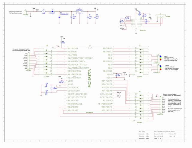
This document provides information for developing a Vehicle Accessory Computer Interface (VACI). The project involves a straightforward design that required approximately three weeks of planning, programming, and debugging. The interface has garnered significant interest, with many users expressing a...
Accessories built so far include a linear power supply, a switch-mode power supply, a tuning aid, and a headset. An antenna tuner and SWR meter will be described later. To operate the new transceiver, a power supply was needed....
This project builds upon the 2012 LED Flicker project. The objective is to create an ultra-bright, multi-channel test light using high-power LEDs driven to their maximum rated current with precise control. By utilizing an array of seven ultra-bright LEDs,...