
printed circuit board pcb etching

The construction of a printed circuit board (PCB) using the toner transfer method involves several critical steps that require careful attention to detail. Initially, the design phase begins with the schematic capture, where the circuit's functional aspects are mapped out using electronic CAD software. In this instance, Eagle was selected due to its accessibility for small projects and the wealth of online support available. The layout of the PCB is crucial, as it dictates the placement of components and the routing of traces. The auto-router feature in Eagle can facilitate this process, but manual adjustments are often necessary to optimize trace routing and avoid potential issues such as trace interference or inadequate spacing.
Once the layout is finalized, the next step is to prepare the transfer medium. While glossy or photo paper is typically recommended for the toner transfer process, alternative materials such as glossy magazine paper can also yield successful results. The principle behind this method relies on the unique properties of laser toner, which adheres more effectively to certain surfaces when heat is applied. The PCB substrate is then cleaned to ensure good adhesion of the toner during the transfer process.
The application of heat is a critical phase in this method. The clothes iron must be preheated, and the circuit pattern printed on the chosen paper is placed face down onto the copper-coated board. Careful pressure is applied, ensuring even contact to facilitate the transfer of the toner. It is essential to avoid moving the iron too much during this process to prevent smudging of the circuit pattern. After the transfer, the paper is removed, revealing the toner pattern on the copper surface.
Following the successful transfer, the PCB undergoes an etching process to remove the unprotected copper, leaving behind the desired circuit traces. This step typically involves submerging the board in a ferric chloride solution or a similar etchant, which selectively removes the copper not covered by toner. Once etching is complete, the board is cleaned, and the toner can be removed using a suitable solvent, revealing the copper traces that will form the electrical pathways of the circuit.
The final steps include drilling holes for component placement and soldering the components onto the board. This process requires precision to ensure that each component is correctly oriented and connected according to the original schematic. Testing the completed circuit is crucial to verify that all connections are functioning as intended before finalizing the project. This method of PCB fabrication, while requiring practice and patience, ultimately enables the creation of custom electronic circuits tailored to specific project needs.This post assumes some knowledge of PCB etching methods and is an account of my experience with the toner transfer method. If this is new to you, you may have to get Googling on a few of things mentioned here. That said, I`ve linked to the sites I found most useful during the process. It`s a fairly straightforward process to build the circuit on a piece of protoboard, and for an Electric Window 3 circuit, it takes about two hours. The bottleneck of this process is preparing all the connecting wires (shown in white in the above photo) and ensuring all the interconnections are correct, ie, connecting the right components to the right pins of the microprocessor and the power and ground points. For our recent contribution to the Chinatown Remixed exhibition, Deb and I (working as The Latest Artists ) envisioned a series of Electric Window 3 light boxes, displaying various animations along with text from Twitter via a wireless internet connection.
I decied to use this as an opportunity to finally learn how to etch PCBs. There seemed to be a steep learning curve, as I`d yet to use electronic CAD software such as Eagle, and the actual etchning process seemed finicky and messy. After watching Collin`s video, a few others on YouTube, and reading some on-line tutorials (found via Google), I decided to attempt etching with the toner transfer method, since I already have a laser printer and clothes iron.
I knew I`d be creating a single-sided board for the sake of simplicity, so I created a rough layout by hand ” based on my existing hand-drawn schematic (not shown) ” to get an idea of where the components should best be and which microprocessor pins were best to avoid crossing wires and/or requring jumpers: While there are plenty of software alternatives, free and otherwise, for schematic capture and PCB layout, I decided to go with Eagle because a) it`s free to use for 3 ³ x 4 ³ boards, and b) there`s an abundance of resources/help out there for it. I then moved onto the PCB layout portion and used the auto-route feature to start the intimidating process of trace layout.
With a bit of additional tweaking by hand, I had a layout I was happy with. I originally designed the board to be 3 ³ x 1. 5 ³ but that resulted in tight traces and traces running really close to microprocessor pin connections. Being unsure of the tolerances/accuracy of the etching process to come, I decided to give the circuit more margin and ended up with a 3 ³ x 2 ³ board: Although I`d repeatedly read that glossy or photo paper was best to print the circuit for transfer onto the copper board, I didn`t have any of these fancy papers on hand, and didn`t want to make a trip to the store if I didn`t have to.
So I decided to try it with regular paper. Naturally I didn`t turn it on until resting it on its back, and I wish more turorials were explicit about whether or not you should have water in there or not. The answer is no. and it didn`t work. After several attempts to iron the circuit pattern onto the pattern from regular paper, it just wouldn`t stick.
Whenever I`d move the iron around, the paper would slip and the result would be a smugged circuit pattern on the copper board. I really didn`t want to make a run to the store for special paper, so I consulted Google instead. I found this great article explaining how you can use glossy magazine paper, the principle being that the laser toner doesn`t stick very well to it, thus making it easy to transfer onto the copper ” the same principle behind using special glossy or photo paper I`d previously read about.
I set to work with the cheaper and more easily available magazine paper I already had around, trimming it to fit my printer before making a few prints of the circuit: and it stuck! The paper stuck pretty much immediatly after applying heat with the iron, and I was able to move the iron around and evenly heat the entire circuit.
Soon I could see the traces 🔗 External reference
Related Circuits
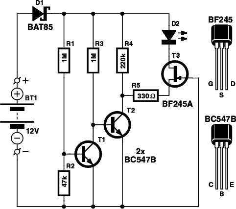
The i-TRIXX circuit is designed to prevent issues for individuals traveling in a caravan. It provides an early warning system through an illuminated LED, alerting users when the battery charge is low, thereby preventing the inconvenience of being unable...
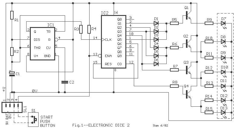
The IC1 is a 555 timer IC connected for astable operation. The clock pulses are fed to the IC2 via the 10K resistor. The IC2 is a 10-stage counter; output 6 (pin 5) is connected to RESET (pin 15),...
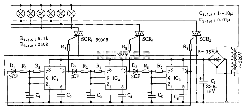
The circuit utilizes a 555 timer as its core component to control three lights through a cyclic trigger monostable delay circuit. The brightest light is controlled by a silicon-controlled rectifier (SCR) that determines the cycle of illumination. When pin...
Certain circumstances and areas require the detection and securing of entrance paths through alarm systems, ensuring that whenever an individual opens an entrance door, the situation is instantly monitored by triggering an alarm. Battery-operated window and door alarms are...
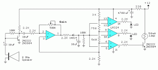
This decibel meter circuit responds to sound pressure levels ranging from approximately 60 to 70 dB (decibels). The sound is captured by an 8-ohm speaker and amplified using a transistor stage along with an LM324 operational amplifier section. A...
The human ear can detect sounds ranging from 20Hz to 20KHz, with the normal range typically between 100Hz and 13KHz, depending on an individual's age and health. For accurate measurements, a range of 20Hz to 20KHz is used. Sounds...