
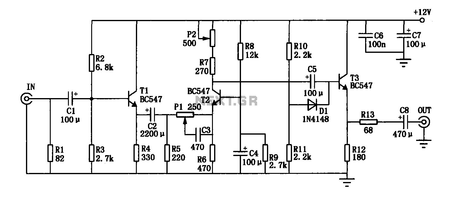
Pure CL B amplifier circuit
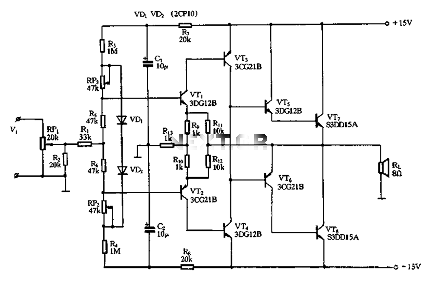
The described circuit effectively stabilizes the operating conditions of the transistors through the use of temperature compensation and biasing techniques. The inclusion of diode VDi serves as a critical element in maintaining the base bias for VTi and VT2, which is essential for ensuring reliable transistor operation across varying supply voltages. The temperature stability offered by the circuit is particularly important in applications where ambient conditions may fluctuate, as it prevents performance degradation that could arise from thermal drift.
Capacitors C1 and C2, in conjunction with resistor R7, play a vital role in filtering out unwanted noise from the input signal. This noise reduction is crucial for high-fidelity audio applications, where any hum or interference can significantly impact sound quality. The experimental findings highlight the importance of this filtering stage, demonstrating that the circuit's performance can vary dramatically based on whether this filtering is implemented.
The quasi-complementary push-pull output stage formed by transistors VT3 through VT8 is designed to operate efficiently in a Class B configuration. This configuration is advantageous for audio amplification as it minimizes power dissipation during idle periods, thereby enhancing overall efficiency. The careful calibration of the output stage ensures that the transistors remain off when no signal is present, which is critical for preventing crossover distortion that can occur in push-pull amplifiers.
During the debugging process, the use of a multimeter allows for precise monitoring of output current, ensuring that adjustments to the circuit do not lead to unintended consequences. Setting RP3 to maximum resistance and adjusting RP2 and RP3 to achieve a zero output current serves as a methodical approach to calibrating the circuit, ensuring that it operates within the desired parameters. The target supply current of 2 to 2.5 mA is indicative of the circuit's readiness for optimal performance, balancing power consumption with the need for effective amplification. Circuit, the diode VDi, f Pooh is used to stabilize VTi, VT2 base bias, so that when the supply voltage in a certain range, VTi, VT2 a more stable quiescent point. If there is a temperature change at the same time, since the two grant tube PN junction transistor PN junction temperature changes and changes in the same direction, can play a role in compensation, protection temperature stability of the circuit. C1, R7 and C2, who constitute the input stage bias strip of filter networks to reduce hum noise input circuit.
Experiments show that the circuit access or not, the effect is quite different. VTs ~ VT8 constituting the composite quasi-complementary push-pull output stage, has been adjusted so that the static Jo /C4, therefore, in the absence of the letter when, and outputs the tubes are in the OFF state, that is pure B state. When a signal is output VT3, VT4 the form of a current applied to the VTs, VT6 base, thus avoiding the post due to the transistor input voltage dead zone caused by the distortion.
Circuit debug: two people are the power multimeter a string, a string of people between the output terminals and the speaker will RPi rotation to ground, build) 2, RP3 maximum resistance to rotation end power. While adjusting RP2, RP3t and adjusted so that the process has remained the string table in the output circuit current reading is zero.
When adjusted to supply current table is 2- 2 5mA to o
Related Circuits
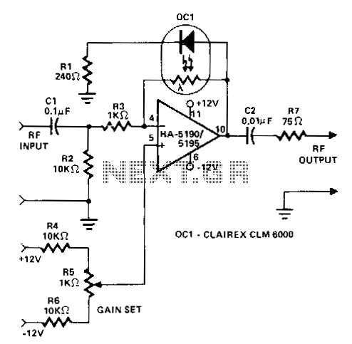
This circuit operates as a wideband adjustable automatic gain control (AGC) amplifier. It has an effective bandwidth of approximately 10 MHz and can handle RF input signal frequencies ranging from 3.2 to 10 MHz at levels between 40 mV...
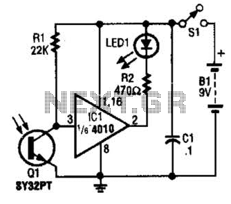
The IR Tester circuit indicates whether the button pressed on a remote control is functioning. Q1 is a phototransistor that is activated by infrared (IR) energy. The IR Tester circuit operates by detecting infrared signals emitted by remote control devices...
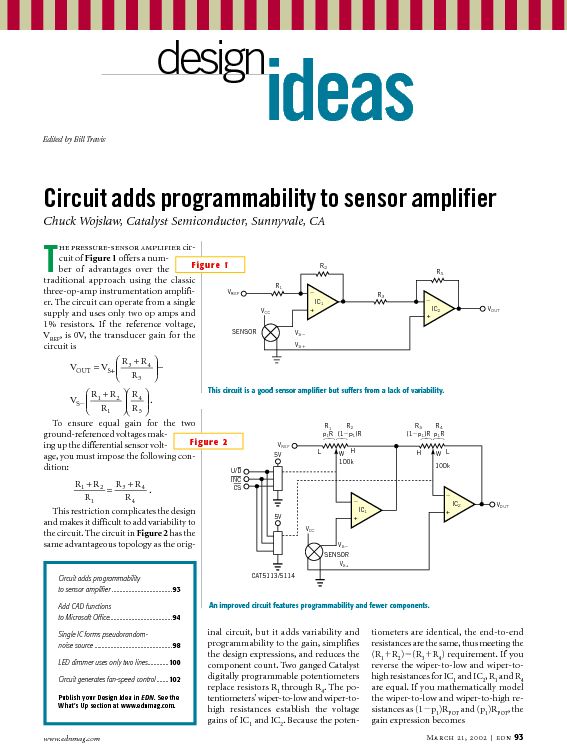
This tutorial provides information related to sensor amplifiers, schematics, and noise. It presents a discussion around sensors and their outputs. Sensor amplifiers are critical components in various electronic systems, especially in applications where signals from sensors need to be conditioned...
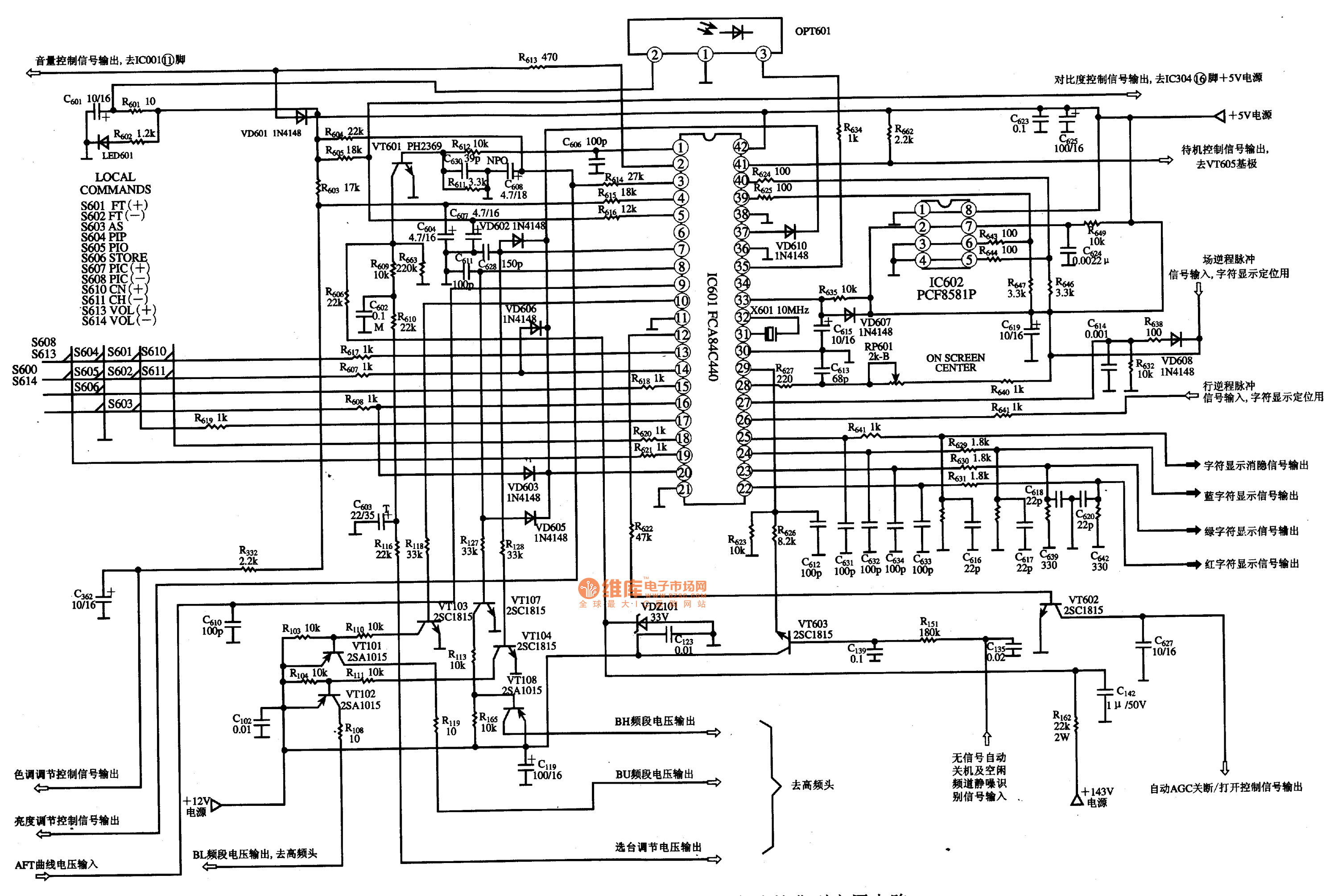
The PCA84C-440/441 is a single-chip microcomputer integrated circuit produced by Philips. It is widely utilized in both domestic and imported large screen color televisions, including those manufactured by Philips and other brands. The PCA84C-440/441 IC is housed in a...
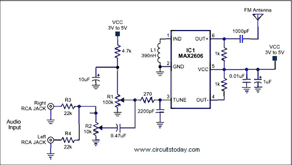
A simple single-chip FM transmitter circuit with a diagram and schematic using the IC MAX 2606, which is a high-performance voltage-controlled oscillator (VCO). The FM transmitter circuit utilizing the MAX 2606 is designed for efficient frequency modulation of audio signals....
The enhancement circuit, as depicted, increases the high-frequency components of the video signal, thereby improving the contrast of the television image. It can be connected between the VCR and the TV SCART input. The circuit utilizes transistor T1 for...