
Quartz Crystals

The crystal oscillator circuit is a critical component in various electronic devices, serving as a stable frequency reference. The design of such a circuit must consider several key parameters to ensure optimal performance. The drive level, which indicates the maximum power that can be applied to the crystal unit without causing damage, plays a pivotal role in the reliability of the oscillator. Operating the crystal beyond its specified drive level can lead to a reduction in the quality factor (Q factor), resulting in poorer frequency stability and potential failure of the crystal itself.
The load capacitance (CL) is another vital aspect of the oscillator design. It directly influences the oscillation frequency, as the crystal's resonant frequency is affected by the capacitive loading. The effective load capacitance must be matched with the specified load capacitance of the crystal to achieve the desired frequency accuracy. This matching process is crucial, as any mismatch can lead to frequency drift or instability.
To ensure stable oscillation, the circuit must be designed so that the negative resistance is sufficiently greater than the equivalent series resistance (ESR) of the crystal. This condition ensures that the circuit can sustain oscillation. An adequate oscillation allowance, defined as the ratio of negative resistance to equivalent series resistance, should be at least five times to guarantee reliable operation.
The inclusion of a series resistor, designated as "Rx," provides an adjustable means to control the starting and stopping of oscillation. By gradually varying the value of Rx, the effective negative resistance can be fine-tuned. The effective resistance "Re" is added to this maximum resistance to determine the overall negative resistance of the circuit.
Finally, it is imperative to consider the temperature coefficient of the crystal and its operating range. Frequency variation is typically more pronounced over wider temperature ranges, necessitating careful selection of components and design strategies to minimize drift and maintain accuracy. Proper thermal management and compensation techniques may be required to ensure that the oscillator performs reliably across its intended operating conditions.The drive level of a crystal unit is shown by the level of the operating power or the current consumption (see Figures 9, 10, and 11). Operating the crystal unit at an excessive power level will result in the degradation of its characteristics, which may cause frequency instability or physical failure of the crystal chip.
Design your circuit within absolute maximum drive level. The load capacitance (CL) is a parameter for determining the frequency of the oscillation circuit. The CL is represented by an effective equivalent capacitance that is loaded from the oscillation circuit to both ends of the crystal unit (see Figure 12). The oscillation frequency varies depending upon the load capacitance of the oscillation circuit. In order to obtain the desirable frequency accuracy, matching between the load capacitances of the oscillation circuit and the crystal unit is required.
For the use of the crystal unit, match the load capacitances of the oscillation circuit with the load capacitances of the crystal unit. To ensure stable oscillation, the negative resistance of the circuit should be significantly larger than the equivalent series resistance (the oscillation allowance is large).
Ensure that the oscillation allowance is at least five times as large as the equivalent series resistance. Add resistor "Rx" to the crystal unit in series and ensure that the oscillation starts or stops. The approximate negative resistance of the circuit is the value obtained by adding the effective resistance "Re" to the maximum resistance "Rx" when the oscillation starts or stops after gradually making Rx value larger.
Please make sure to consider the temperature range and frequency accuracy you need since magnitude of frequency variation becomes larger and larger as the temperature range becomes wider. 🔗 External reference
Related Circuits

This is a simple automatic light switch circuit designed for bedrooms. After construction, connect the input terminals of this circuit in parallel to the existing light fixture. The automatic light switch circuit operates using a photoresistor (LDR) and a transistor...
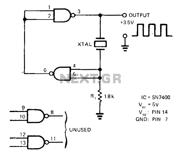
A SN7400 quartz crystal and a resistor provide a square-wave output of approximately 3.5 V. The circuit operates reliably at frequencies from 120 kHz to 4 MHz. The circuit utilizes a SN7400 integrated circuit, which is a quad two-input NAND...
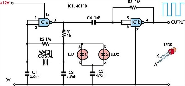
This circuit was designed to enable the use of watch crystals in an existing CMOS oscillator circuit powered by a 12V supply. The challenge arises because these crystals typically operate at a maximum supply voltage of approximately 6V; exceeding...
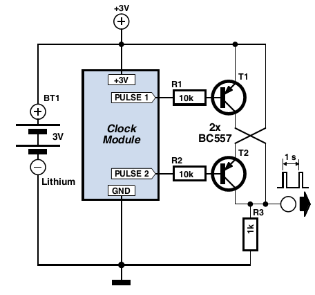
Many electronic projects require a timebase generator that is accurate to within a second. One method of achieving this is through the use of a microcontroller, quartz crystal, and appropriate software. However, a more cost-effective and straightforward approach is...
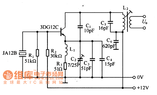
The 27MHz quartz crystal oscillator circuit is illustrated in figure 1. The biasing circuit consists of resistors R1, R2, and R3, while C6 serves as the bypass capacitor. The partial voltage circuit includes capacitors C1, C2, C3, and C4...
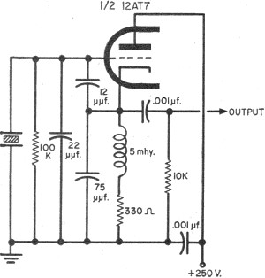
To update the fundamental oscillator circuits, simply replace the transistors with tubes. Alternatively, if one owns a vintage vacuum tube radio, it may be of interest to learn about historical practices. In general, the foundational principles of electronic circuits...