
Quick-Charge Auto-Fire Flash Circuit
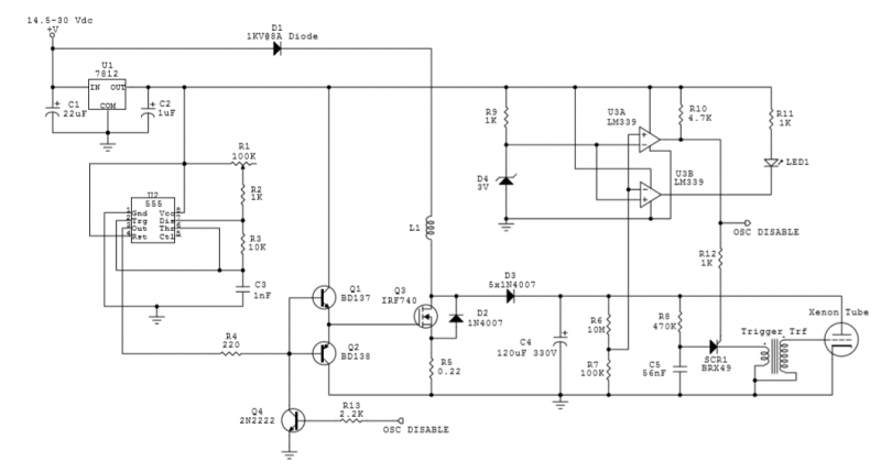
It features specialized gate drive circuitry consisting of transistors Q1 and Q2, which facilitate rapid turn-on and turn-off. L1 is a hand-wound inductor wrapped around a small ferrite rod, with an inductance of approximately 135 µH. Capacitor C4 is charged through diode D3, and once the capacitor voltage slightly surpasses 300V, the auto-charge circuit takes control. Comparator U3A outputs a high signal, while U3B outputs a low signal. The output from U3A is used to trigger the SCR (BRX49) and activate transistor Q4. Consequently, the oscillator pulses do not reach the MOSFET gate drive circuitry, effectively turning the MOSFET off. Otherwise, the inverter could charge the capacitor to about 500V, which would damage it. Diode D3 consists of five 1N4007 diodes in parallel to accommodate the charging current, which can peak at several amperes. Meanwhile, capacitor C5 is charged through resistor R8. When the SCR is activated, all energy stored in C5 is released into the primary of the trigger coil, generating several kilovolts of high voltage output at the secondary. The secondary lead is directly connected to a Xenon tube, ionizing the gas inside. Once ionized, the gas becomes a conductive path, allowing C4, charged to 300V, to discharge through the flash tube, producing an intense flash. The SCR driving current is supplied by C5, and since R8 is a large resistor that drains current below the SCR's holding current, the SCR turns off after each discharge. C4 begins to recharge, and this cycle repeats.
The flash firing rate is dependent on the DC supply voltage, the oscillator frequency, and the duty cycle set by R1. As the supply voltage increases, the flash rate accelerates. Observations indicate flash rates of approximately four to five flashes per second (fps) at a DC source of 24V, which is 16-20 times faster than a single-shot circuit (which requires 4 seconds per charge). When powered by 12V, the flash rate decreases to about 1-2 fps, and this can be further reduced by adjusting R1. Although R5 is included to sample the source current, it can be omitted. The flash rate diminishes as the MOSFET heats up, resulting in lower drain current and reduced kickback voltage, particularly noticeable at higher DC supply voltages. Consequently, the amount of kickback voltage decreases, leading to slower charging.
The circuit is designed to efficiently manage high-voltage discharges while ensuring the safety and longevity of its components. The use of the IRF740 MOSFET allows for higher inductive kickback handling, while the gate drive circuitry ensures rapid switching, crucial for maintaining the desired flash rate. The implementation of the SCR adds a layer of control over the discharge cycle, allowing for precise timing and energy management in the flash generation process. Overall, this circuit represents a well-engineered solution for high-voltage flash applications.The circuit uses an IRF740 MOSFET which is rated at a maximum DS V value of 400V. The avalanche voltage is calculated as 3520 1. max DSA VV V. This means that up to about 500V of inductive kickback voltage can develop in the switched coil. More than that will cause the avalanche effect, and turn the MOSFET on. For example, IRF640 doesn’t work well with this design because the maximum kickback voltage that can be obtained is about 250V. So I selected IRF740 for this application.
It has a special gate drive circuitry consisting Q1 and Q2 for fast turn-on and turn-off. L1 is a hand-wound inductor around a small ferrite rod. Its inductance is about 135 µH. C4 is charged through D3, and when the cap voltage slightly exceeds 300V, the auto-charge circuit takes the control. Comparator U3A generates a high output, and U3B generates a low output. The U3A output is used to trigger the SCR (BRX49) and to turn-on Q4.
Hence the oscillator pulses do not reach the MOSFET gate drive circuitry.
This effectively turns the MOSFET OFF. Otherwise, the inverter is capable of charging the cap up to about 500V, and this will sure blow the cap! D3 is five 1N4007s in parallel since the charging current has peak value of several amperes. Meanwhile, C5 is charged through R8. Once the SCR is turned on, all the energy of C5 is dumped on the trigger coil primary and several KVs of high voltage output is generated at the secondary.
The secondary lead is directly connected to the Xenon tube and will ionize the gas inside. Now the gas is ionized, becomes a conductive path, and C4 charged to 300V discharges through the flash tube causing an intense flash. Since the SCR driving current is provided by C5, and since R8 is a very large resistor and drains a current less than the SCR holding current, SCR turns off after each fire.
C4 starts charging again, and this cycle continues.
The firing rate for the flash depends on the dc supply and, the oscillator frequency and the duty cycle (as set by R1). As the supply voltage gets higher, the flash fires faster. I have observed flash rates of about four-five flashes per second (fps) when the dc source was 24Vdc.
That is 16-20 times faster than the single-shot circuit (4 sec per charge). However, when the circuit was fed by 12Vdc, the flash rate was reduced to about 1-2 fps. It can be made even slower by adjusting R1. This is still a good achievement, if not a breakthrough. R5 can be omitted because it is placed to sample the source current. The flash rate decreases as the MOSFET gets hot (lower drain current and lower kickback voltage). This is more evident especially at higher dc supply voltages. The amount of kickback voltage is reduced and charging becomes slower. By 4beowulf7 - [email protected]
Related Circuits
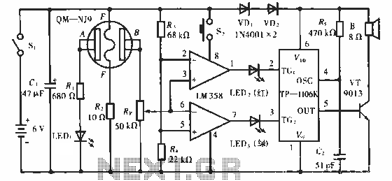
The QM-NJ9 is an alcohol sensor that detects the presence of alcohol by measuring the resistance values between points A and B. When alcohol is detected, the resistance decreases, leading to an increase in potential at point B. As...
The metal detector circuit is presented here, illustrating a simple yet effective design. It utilizes a 40, 106 Hex Schmitt inverter IC, a capacitor, a search coil, and batteries. An advantage of connecting IC1b Pin 4 to a medium-wave...
The video amplifier circuit utilizes the LM359 integrated circuit, which is a dual, high-speed, programmable current mode (Norton) amplifier. This circuit is suitable for general-purpose video amplification applications. The LM359 is designed to operate as a high-speed amplifier, making it...
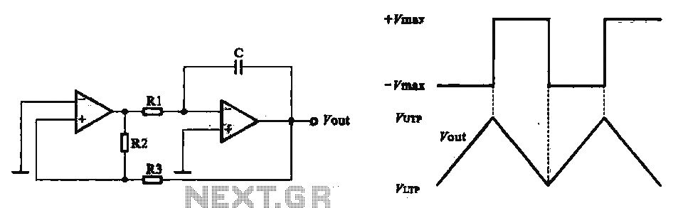
This circuit utilizes two operational amplifiers configured as triangular wave oscillators. It demonstrates a practical application of a relaxation oscillator that employs a voltage comparator to execute the switching function. The schematic in FIG. 2 illustrates the composition of...
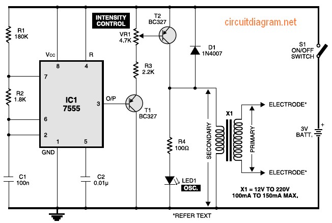
Figure 1 shows the circuit of a muscular stimulator. The IC 7555 is configured as an astable multivibrator to generate approximately 80Hz pulses. The output from IC1 is connected to transistor T1, whose emitter is linked to the base...
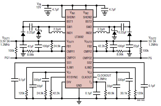
The LT3692 dual current mode PWM step-down DC-DC converter circuit, featuring two internal 3.5A switches, can be designed into a simple power supply circuit suitable for various electronic applications, such as distributed supply regulation or automotive circuits. The LT3692...