
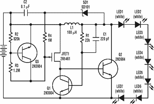
R/C Airplane LED Flasher


I used the AVR ATTINY12 controller from Atmel because I have plenty left over from other projects. With some modification to the code, you can use the ATTINY13, which is also available in both 8 pin DIP and surface mount packages, or nearly any AVR or other small CMOS controller. See firmware discussion below.
Here is the pin assignment for the ATTINY12 and ATTINY13.
Pin 1 Battery +
Pin 2 PORTB3 4 Hz, 50 ms positive pulse
Pin 3 PORTB4 10 Hz 50 ms positive pulse (square wave)
Pin 4 Battery -
Pin 5 PORTB0 4 Hz 100 ms positive pulse
Pin 6 PORTB1 2 Hz 50 ms positive pulse
Pin 7 PORTB2 4 Hz 100 ms positive pulse
Pin 8 Battery +
The "heartbeat" of the firmware is a subroutine named wait_50ms which sets up the 8-bit timer to interrupt the processor, and then puts the processor to sleep. After 50 milliseconds, the processor is awakened by the timer interrupt, the interrupt is cleared, and the subroutine returns to the instruction in the main routine after the instruction that called wait_50ms.
The main routine merely sets or clears bits on the output pins and then waits for 50 milliseconds, and sets and clears pins as appropriate to reproduce the intended waveforms on the output pins. Since there is only one timing routine, all changes on the output pins take place according to the 50-millisecond granularity of this timing method. It should be noted that because there are varying numbers of instructions between calls to wait_50ms, the timing between changes in the output pins varies throughout the entire 1-second cycle by a few microseconds. This tiny variation in timing is not visible. Using this method to control the timing of the drive pulses brings a new meaning to the term "flash memory".
You may notice that pin 5 has the same pattern as pin 7. Each pin drives a 50-millisecond pulse at 4 Hz. The pulses from the two pins are synchronized and in phase. On an ATTINY12, each pin can supply up to 40 milliamps, for a total of 80 milliamps to drive the LEDs.
The internal clock for the ATTINY12 is 1.2 MHz while the internal clock for the ATTINY13 can be either 4.8 MHz or 9.6 MHz. If you use the ATTINY13, you will have to either accept that the flashes will be at a higher frequency and a shorter duration, or modify the code to take into account that higher clock speed. It may also be necessary to modify the setup of the timer in the ATTINY13.
The circuit utilizes a compact design to minimize weight while ensuring efficient operation within the specified voltage range. The ATTINY12 or ATTINY13 microcontrollers serve as the central processing unit, executing the programmed firmware that controls the LED flashing sequences. The power supply is connected to pins 1 and 8, providing the necessary voltage to the microcontroller and the LEDs.
Output pins (PORTB0, PORTB1, PORTB2, PORTB3, and PORTB4) are configured to generate specific pulse widths and frequencies, allowing for the desired LED flashing patterns. The use of a timer interrupt allows for accurate timing control, ensuring that the LED flashes occur at the intended intervals without excessive power consumption.
The design must consider the maximum current output of the microcontroller pins while ensuring that the total current draw remains within the limits of the battery capacity. The firmware's efficiency is crucial in maintaining low power consumption, particularly given the limited battery resources available in the Parkzone Citabria. The synchronization of the output pins enhances the visual effect of the flashing LEDs, providing clear visibility during flight.
Overall, this LED flasher circuit effectively meets the design constraints of weight, power consumption, and voltage requirements while delivering a functional and visually appealing solution for R/C airplane enthusiasts.This was designed to flash a pair of LEDs to be mounted on the wing tips of a Parkzone Citabria R/C (remote control) airplane. The unmodified Parkzone Citabria only weights 20 grams (about 0.7 oz), so weight, and therefore the number and size of the electrical components for the flasher are critical.
Another major constraint was the range of power supply voltage and current draw. The battery in the Parkzone Citabria varies from 3.7 to 4.2 volts. which rules out circuits such as the Simplest LED Flasher Circuit, which requires a higher voltage. Current draw also needs to be kept low because the battery is tiny. The CMOS AVR controller handles both of these requirements beautifully. I used the AVR ATTINY12 controller from Atmel because I have plenty left over from other projects. With some modification to the code, you can use the ATTINY13, which is also available in both 8 pin DIP and surface mount packages, or nearly any AVR or other small CMOS controller. See firmware discussion below. Here is the pin assignment for the ATTINY12 and ATTINY13. Pin 1 Battery + Pin 2 PORTB3 4 Hz, 50 ms positive pulse Pin 3 PORTB4 10 Hz 50 ms positive pulse (square wave) Pin 4 Battery - Pin 5 PORTB0 4 Hz 100 ms positive pulse Pin 6 PORTB1 2 Hz 50 ms positive pulse Pin 7 PORTB2 4 Hz 100 ms positive pulse Pin 8 Battery + The "heartbeat" of the firmware is a subroutine routine named wait_50ms sets up the 8 bit timer to interrupt the processor, and then puts the processor to sleep.
After 50 milliseconds, the processor is awakened by the timer interrupt, the interrupt is cleared, and subroutine returns to the instruction in the main routine after the instruction that called wait_50ms . The main routine merely sets or clears bits on the output pins and then waits for 50 milliseconds, and sets and clears pins as appropriate to reproduce the intended wave forms on the output pins.
Since there is only one timing routine, all changes on the output pins take place according to the 50 millisecond granularity of this timing method. It should be noted that because there are varying numbers of instructions between calls to wait_50ms, the timing between changes in the output pins varies throughout the entire 1 second cycle by a few microseconds.
This tiny variation in timing is not visible. Using this method to control the timing of the drive pulses brings a new meaning to the term "flash memory". You may notice that pin 5 has the same pattern as pin 7. Each pin drives a 50 millisecond pulse at 4 Hz. The pulses from the two pins are synchronized and in phase. On an ATTINY12, each pin can supply up to 40 milliamps, for a total of 80 milliamps to drive the LEDs.
The internal clock for the ATTINY12 is 1.2 MHz while the internal clock for the ATINY13 can be either 4.8 MHz or 9.6 MHz. If you use the ATTINY13, you will have to either accept that that the flashes will be at a higher frequency and a shorter duration, or modify the code to take into account that higher clock speed into account.
It may also be necessary to modify the setup of the timer in the ATTINY13. 🔗 External reference
Related Circuits
A low power, long-life LED flashlight circuit. Electronic Design proposed a simple circuit to resolve this in a recent article. The front end of their circuit draws less than a milliamp of extra current. The described LED flashlight circuit is...
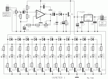
This circuit provides a simple visual indication of audio level signals, adaptable to various user requirements. It can be configured for different input levels, which can be adjusted using trimmer potentiometers TR1 (state) and TR2 (gain). The audio signals...

This kit includes fully illustrated instructions and a circuit schematic. Components are adequately spaced for easy assembly and value identification on the board. The circuit board features silk-screened outlines for component placement, and the circuit pads on the solder...
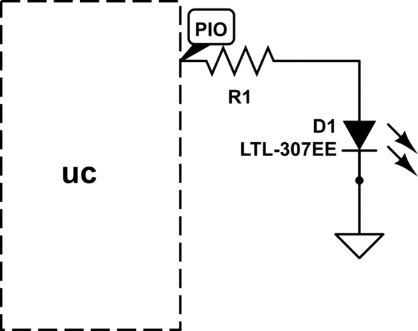
The LED will illuminate when the PIO (Programmable Input/Output) pin goes low, functioning similarly to a ground connection. In this configuration, the current is sourced from the power supply rather than the PIO, as in the first method. It...
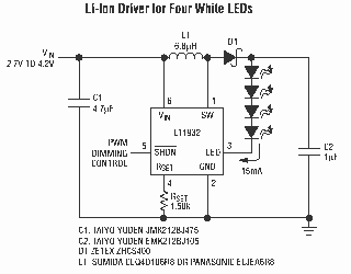
The LT1932 is a fixed frequency step-up DC/DC converter designed to operate as a constant-current source. Because it directly regulates output current, the LT1932 is ideal for driving light emitting diodes (LEDs) whose light intensity is proportional to the...
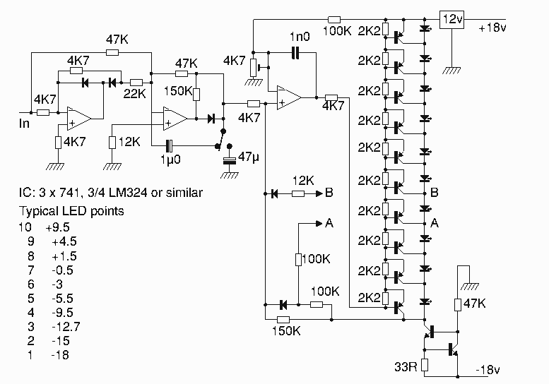
The circuit was designed to work with an audio power amplifier which operated off +18v-0v-18v power rails. The actual voltage used is not too critical except that the feedback is referred to the LED chain which itself is anchored...