
Regulated 12 Volt Supply

The circuit utilizes a 13-volt Zener diode (D2) to achieve voltage regulation, ensuring that the output voltage remains stable at approximately 12.3 volts after accounting for the voltage drop across the base-emitter junction of the transistors, which is typically around 0.7 volts. The configuration allows for a significant output current of up to 500 mA, making it suitable for various applications requiring stable voltage and current.
In this amplified Zener circuit, the Zener diode is connected in reverse bias mode to maintain the desired voltage level. The transistors used in the circuit act as amplifiers, allowing for increased current capacity while maintaining the regulated voltage. The input voltage must be sufficiently higher than the Zener voltage to ensure proper operation, typically requiring a supply voltage that exceeds 13 volts.
The circuit's design also includes bypass capacitors to filter out noise and stabilize the voltage further, enhancing performance in sensitive applications. The output can be connected to various loads, and the circuit's ability to handle 500 mA makes it versatile for powering devices that demand moderate current levels. Proper heat dissipation measures should be considered for the transistors, as they may generate heat during operation, especially under maximum load conditions.
Overall, this circuit represents an effective solution for applications needing reliable voltage regulation with moderate current output, leveraging the properties of Zener diodes and transistors in a compact design.This circuit above uses a 13 volt zener diode, D2 which provides the voltage regulation. Aprroximately 0.7 Volts are dropped across the transistors b-e junction, leaving a higher current 12.3 Volt output supply. This circuit can supply loads of up to 500 mA. This circuit is also known as an amplified zener circuit. 🔗 External reference
Related Circuits
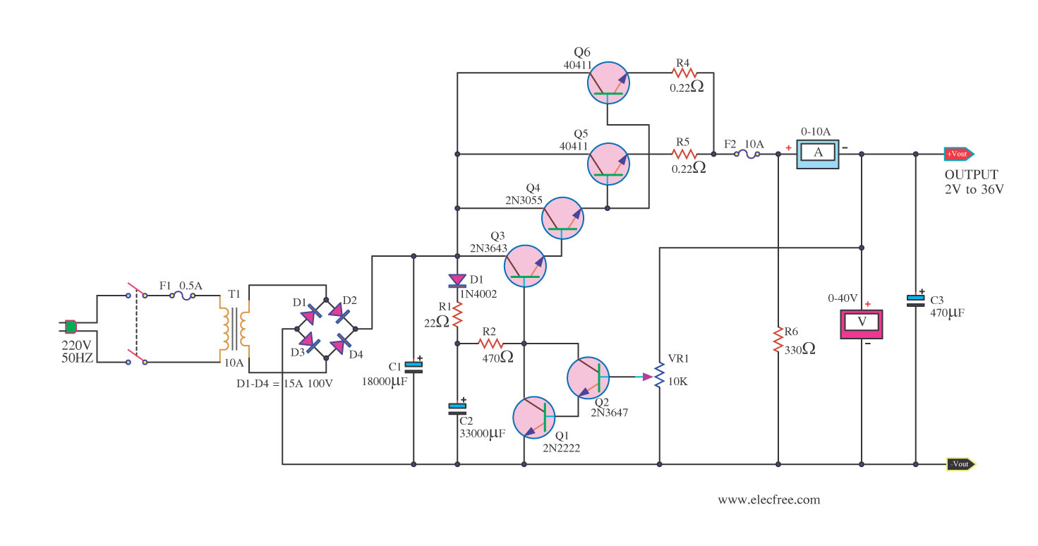
Yesterday, no enhancements were made to the circuit on the blog. Today, a high current power supply capable of delivering 10A has been introduced, featuring an adjustable voltage or variable voltage regulator that can operate within a range of...
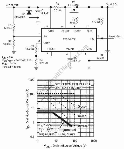
This is a positive high-voltage hot swap controller circuit with a power limiter. This circuit utilizes the TPS2491 or TPS2490, as both of them have specific features. The positive high-voltage hot swap controller circuit is designed to safely connect and...
A circuit is being designed for a DC motor utilizing the following components: 1 x 7805 voltage regulator and 2 x 2N2955 transistors, which are to be paralleled to increase current capacity. The proposed circuit will employ a 7805 voltage...
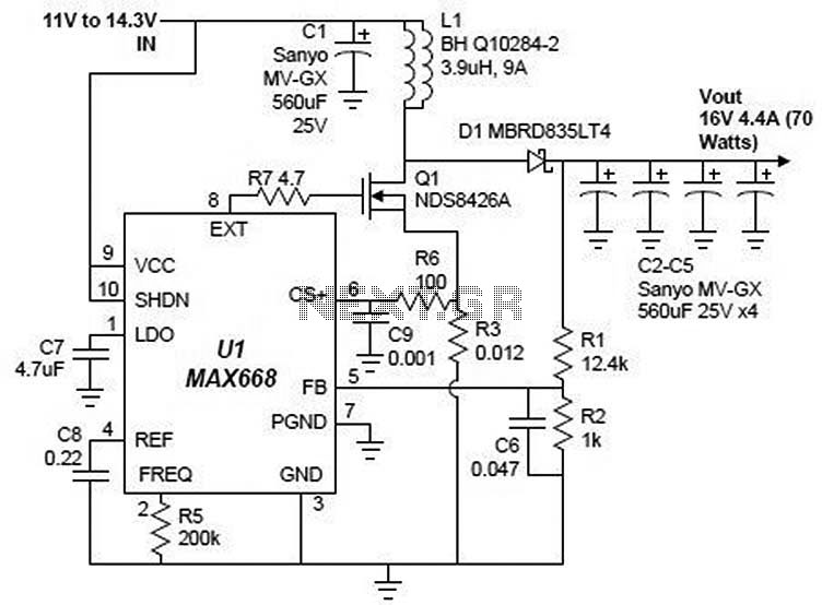
A simple 16-volt switching power supply circuit can be constructed using the provided diagram, which is based on the MAX668 constant-frequency, pulse-width modulating (PWM), current-mode DC-DC controller. This integrated circuit is designed for a wide range of DC-DC conversion...
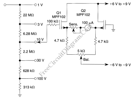
The voltmeter illustrated in the schematic diagram below possesses a very high input impedance. The range selector employs standard voltage divider resistors; however, due to the subsequent preamplifier utilizing JFETs, the divider can be designed with very high resistance...
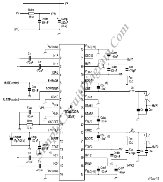
The following circuit diagram illustrates a simplified application circuit for the TDA8932B/33(B) device when it is powered by an asymmetrical supply (single supply). The TDA8932B/33(B) is a class-D audio amplifier integrated circuit designed for efficient audio amplification in various applications....