
Low-Drift High-Impedance JFET DC Voltmeter
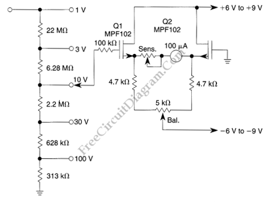
The described voltmeter circuit is engineered for precision measurement of DC voltages, emphasizing high input impedance to minimize the loading effect on the circuit under test. The use of JFETs (Junction Field-Effect Transistors) in the preamplifier stage is crucial for achieving high input impedance, as JFETs inherently possess high gate resistance. This characteristic allows for the use of high-value resistors in the voltage divider without significantly affecting the measurement accuracy.
The voltage divider configuration is essential for scaling down the input voltage to a level suitable for the JFET input stage. The choice of resistors in the divider must be made carefully, considering thermal stability and drift characteristics to ensure consistent performance. The low drift specification indicates that the circuit is designed to maintain accuracy over time and temperature variations, which is critical for precision applications.
The balanced-bridge configuration of the source-follower amplifier, formed by the two matched JFETs, enhances the circuit's performance by ensuring that any common-mode noise is effectively rejected. Matching Q1 and Q2 within 10% for their drain-source saturation current (Idss) is vital for maintaining the balance of the bridge. This matching minimizes offset voltages and improves the overall stability of the circuit, especially under varying environmental conditions.
In summary, this voltmeter circuit is a sophisticated design that leverages high-impedance JFET technology and a balanced-bridge topology to deliver accurate and stable voltage measurements. The careful selection and matching of components are fundamental to achieving the desired performance characteristics, making it suitable for high-precision applications.The voltmeter shown in the schematic diagram below has very high impedance. The range selector uses conventional voltage divider resistors, but since the following pre amplifier uses JFET, the divider can be designed using very high resistance series resistors. This DC voltmeter circuit also featured with low drift. This circuit uses a pair JFETs, which is configured in a balanced-bridge source-follower amplifier circuit. The Q2 and Q1 must be matched within 10% for Idss that will maintains bridge balance over temperature. Here is the schematic diagram of the circuit: 🔗 External reference
Related Circuits
The logic voltage is applied simultaneously to the sample and hold JFETs. By matching input impedance and feedback resistance and capacitance, errors due to the drain-source on-resistance (rdson) of the JFETs are minimized. The circuit employs a sample and hold...
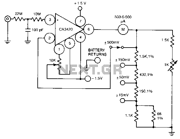
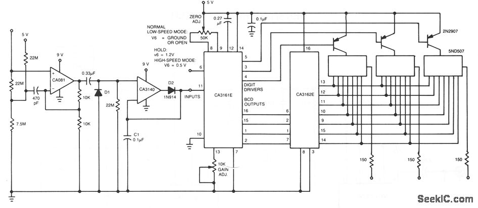
A resistance of 1,000,000 MΩ takes advantage of the high input impedance of the CA3420 BiMOS op-amp. Only two 1.5-V AA-type penlite batteries are required for use. Full-scale deflection is ±500 nV, ±150 mV, and ±15 mV. The circuit utilizes...

A simple linear voltage-controlled amplifier can be constructed with one operational amplifier (op amp) and two junction field-effect transistors (JFETs). This amplifier can achieve an 80-dB dynamic control range with less than ±0.2% linearity error for 0 V. The described...
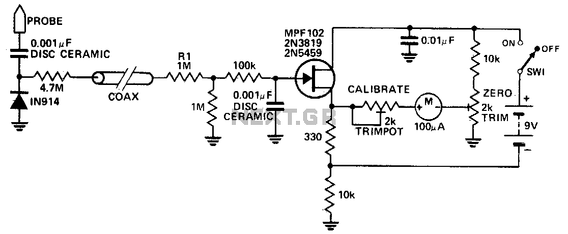
This circuit measures RF voltages exceeding 200 MHz and reaching up to approximately 5 V. The diode must be installed in a remote probe, positioned near the probe tip. The sensitivity is exceptional, allowing for the measurement of voltages...
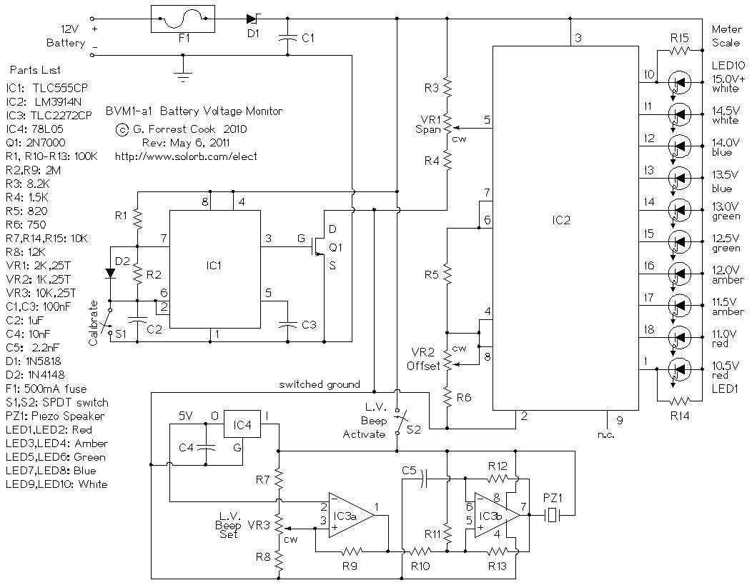
This is a low power voltmeter circuit that can be used with alternative energy systems that run on 12 and 24 volt batteries. The voltmeter is an expanded scale type that indicates small voltage steps over the 10 to...
The CA081 and CA3140 BiMOS operational amplifiers provide minimal loading on the circuits being measured. The wide bandwidth and high slew rate of the CA081 enable the meter to operate at frequencies up to 0.5 MHz. The CA081 and CA3140...