
RF amplifier and filter for 70 MHz

The RF amplifier is designed to enhance signal strength while maintaining signal integrity, particularly in high-frequency applications. By employing noiseless feedback through the drain-gate capacitance, the amplifier minimizes noise contributions that may affect performance. This feedback mechanism is crucial for stabilizing the amplifier's gain and improving linearity.
The inclusion of an inductor in the source lead plays a vital role in creating the necessary 90-degree phase shift between the gate voltage and the channel current. This phase shift is essential for ensuring optimal operation of the amplifier, particularly in applications where phase relationships are critical, such as in RF signal processing and transmission.
The circuit typically consists of a transistor configured in a common-source arrangement, where the input signal is applied to the gate terminal. The drain-gate capacitance provides a feedback path that influences the behavior of the amplifier, while the inductor in the source lead serves to manage the current flow and enhance the amplifier's frequency response.
In practical implementations, careful selection of the inductor value and the characteristics of the feedback network will determine the amplifier's bandwidth, gain, and overall performance. The design must also account for parasitic capacitances and inductances that may arise in high-frequency applications, as these can significantly impact the amplifier's efficiency and stability.
Overall, this RF amplifier design represents a sophisticated approach to achieving high performance in signal amplification, leveraging feedback mechanisms and inductive components to optimize phase relationships and minimize noise.The RF amplifier uses noiseless feedback through the drain-gate capacitance with an inductor in the source lead to provide the necessary 90 degree phase shift between gate voltage and channel current. 🔗 External reference
Related Circuits
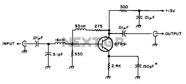
The amplifier delivers a gain of 10 dB across a frequency range of 10-600 MHz and features a 1-to-1 impedance match at 50 ohms. The BFR91 transistor exhibits a noise figure of 1 dB at 500 MHz. The circuit...
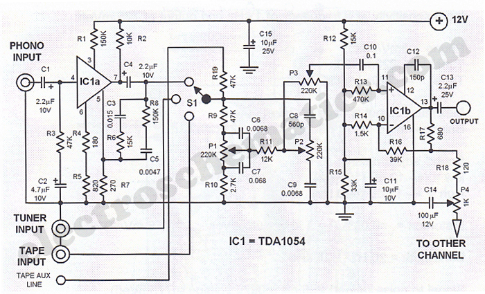
This Hi-Fi stereo preamplifier circuit is designed using the TDA1054 integrated circuit from SGS. The TDA1054 is a 16-pin DIL package that incorporates two separate preamplifier circuits. It is a low-noise preamplifier with minimal complications in the design process....
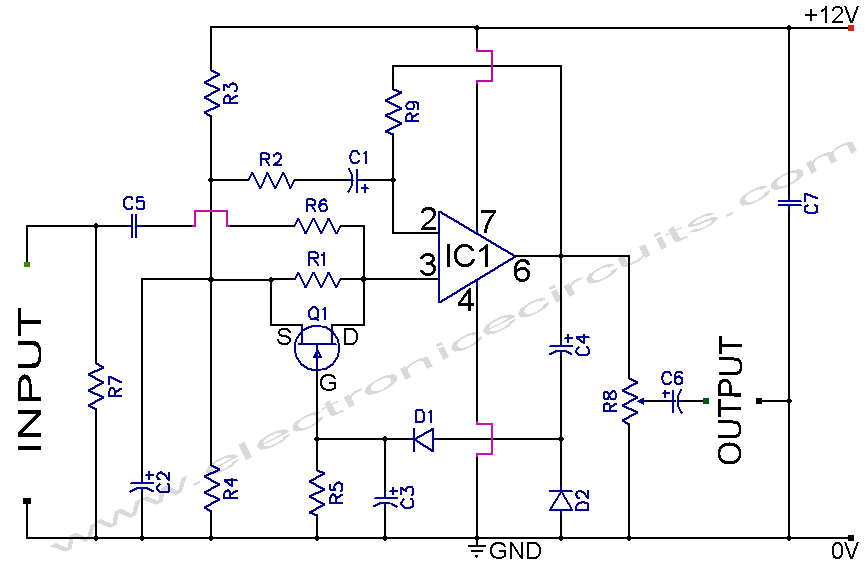
A section of the operational amplifier's output signal is rectified using 1N4148 diodes, followed by filtering, and is then directed to the gate of the FET input shunting circuit. As the output voltage increases, additional input shunting occurs, which...
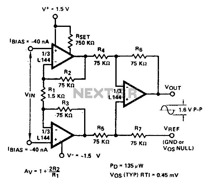
A three-amplifier circuit consumes only 135 µW of power from a ±1 V power supply. With a gain of 101, the instrumentation amplifier is ideal for sensor interface and biomedical preamplifier applications. The first stage provides all of the...
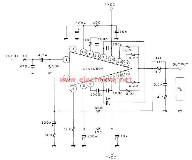
This 200-watt audio amplifier circuit diagram is based on the STK4050V high-power audio amplifier IC, designed to deliver up to 200 watts of audio power on a single channel. The STK4050V 200-watt audio amplifier circuit is pin-compatible with other...
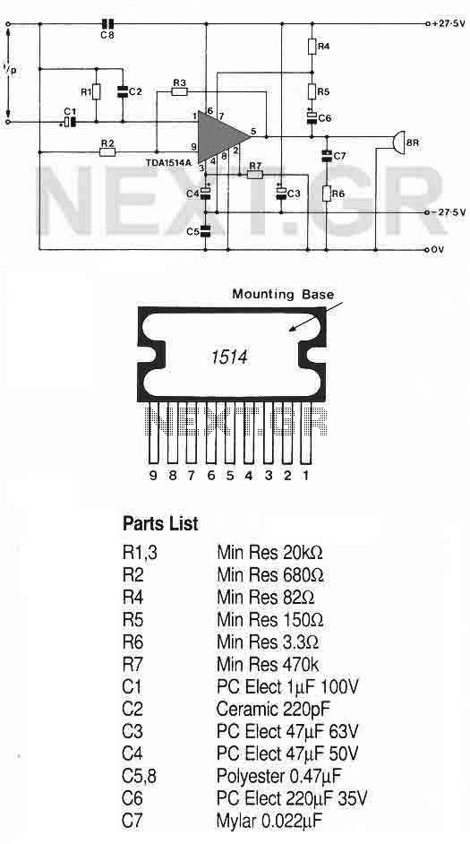
This high-quality audio amplifier is based on the TDA1514A, a 9-pin flat package integrated circuit. The heatsink must be insulated from the ground. The amplifier can deliver 40 watts into an 8-ohm load with a 27.5-volt power rail or...