
RF2103P schematic configuration of 915MHz RF amplifier
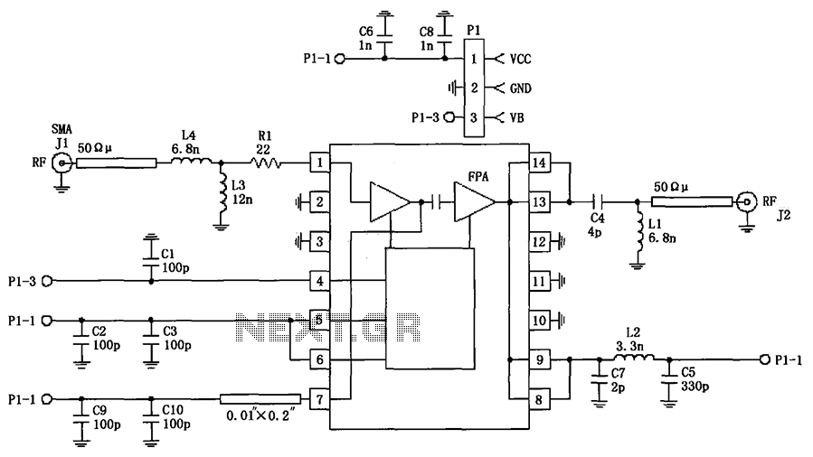
The RF2103P is a high-performance RF amplifier designed for operation at 915MHz, commonly used in various wireless communication applications. The circuit configuration includes several key components that facilitate its operation.
P1, the power connector, is essential for providing the necessary voltage and ground reference to the amplifier. The Vcc connection (P1-1) supplies the required power for the amplifier's operation, while the ground connection (P1-2) ensures stable reference levels for signal processing. The power down control (P1-3) allows for the amplifier to be turned off when not in use, thereby conserving power.
The RF input socket (J1) is where the input signal is fed into the amplifier. This input stage is crucial as it determines the overall performance characteristics, including gain and linearity. The RF output socket (J2) provides the amplified signal to the subsequent stages of the system or to the antenna, depending on the application.
In addition to these primary components, proper impedance matching is vital for maximizing power transfer and minimizing signal reflections at both the input and output stages. This may involve the use of additional passive components such as resistors, capacitors, and inductors to create matching networks tailored to the specific requirements of the 915MHz frequency.
Thermal management is also an important consideration in the design of the RF2103P amplifier circuit. Adequate heat dissipation mechanisms, such as heat sinks or thermal vias, should be implemented to ensure that the amplifier operates within its specified temperature range, thus maintaining reliability and performance.
Overall, the RF2103P 915MHz RF amplifier circuit is a sophisticated design that requires careful consideration of power supply, input/output configurations, impedance matching, and thermal management to achieve optimal performance in wireless communication systems. As shown in FIG constituted by RF2103P 915MHz RF amplifier circuit. P1 for the outlet, which P1-1 take power Vcc, P1-2 ground, P1-3 then power down control voltage VB; J1 to th e RF input socket; J2 as RF output socket.
Related Circuits
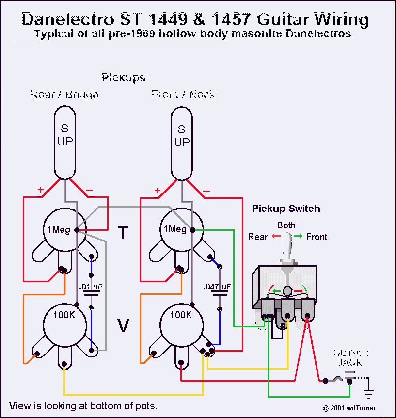
Using a magnetic compass, ensure that both pickups have a South polarity on the top of each pickup. Verify this by checking for a North polarity on the bottom of the pickups. It is uncommon to find both pickups...
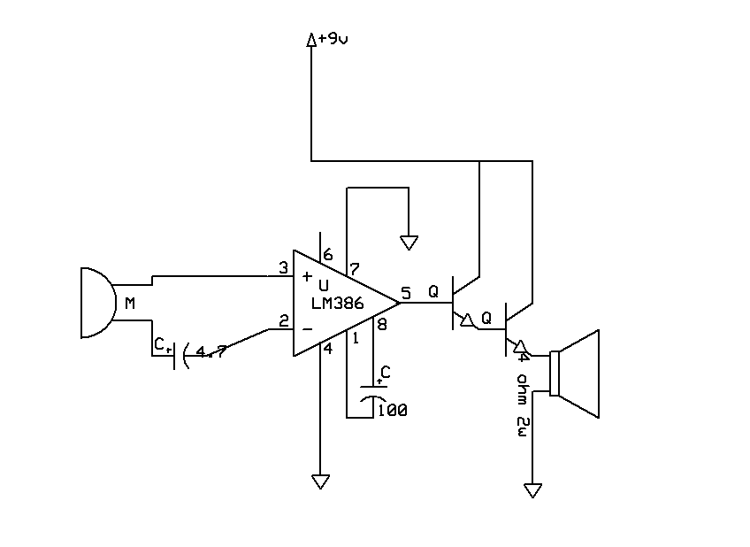
You can use this powerful amplifier in any small audio project. It is very small (6.5 x 4.5 cm). It outputs 10W and uses a 9V battery. More: Components List R1: 6 Ohm R2: 220 Ohm R3: nothing R4:...
A buffered video amplifier is utilized to connect a video player to a receiver or monitor TV over long cable lengths, which may lead to a reduction in signal amplitude and, consequently, a decline in image quality. This amplifier...
The sound quality was poor, and then it stopped functioning. Can anyone explain which part of the circuit may have malfunctioned? Any suggestions to enhance the sound quality and restore functionality? The transistors used are both BC546, and the...
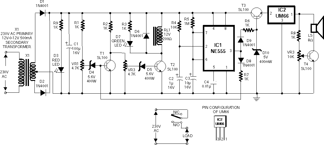
This tiny circuit comprising of a single 3 terminal IC UM66 can be built small enough to be placed inside a greeting card and operated off a single 3V flat button cell. There is not much to the circuit....
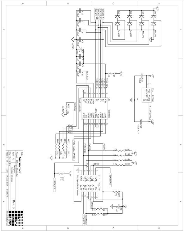
The following are detailed schematics for the QScreen Controller. The QScreen Controller integrates an embedded computer utilizing the 68HC11 microcontroller, along with a touch panel and an LCD (liquid crystal display) graphic user interface (GUI) that is well-suited for...