
Sample-and-hold

The circuit leverages the 8043's low input bias current to minimize the droop effect during the hold phase, ensuring that the output signal remains stable for a significant duration. This is particularly important in applications where maintaining signal integrity during hold periods is critical. The high slew rate of 6 V/µs allows the circuit to respond quickly to changes in the analog input, which is essential for accurately capturing fast signal variations.
In this configuration, the analog input is presented as a ramp signal with a slope of approximately 67 V/ms, which is a common waveform used in testing and calibration scenarios. The sample-and-hold function is triggered by a high logic input, which activates the sampling process. During the sample phase, the output closely follows the input waveform, ensuring that the signal is accurately represented.
The output waveform is intentionally offset by 2 V to provide clear visibility of the relationship between the input and output signals on an oscilloscope. This offset is crucial for preventing trace overlap, which could obscure important details in the waveform analysis. The hold mode is characterized by a constant output that remains unchanged until the next sampling event, allowing for precise measurement and analysis of the input signal.
The time taken for the output to catch up with the input at the beginning of each sample period is approximately 8 µs, which indicates the response time of the circuit. After this initial catch-up period, the output accurately tracks the input signal until the next hold command is issued. This behavior is essential for applications that require precise timing and signal fidelity in analog-to-digital conversion processes or other signal processing tasks.Two important properties of the 8043 are used to advantage in this circuit. The low input bias currents give rise to slow output decay rates (droop) in the hold mode, while the high slew rate at 6 V/p,s improves the tracking speed and the response time of the circuit. The upper waveform is the input 10 V/div, the lower waveform the output 5 V /div. The logic input is high. The center waveform is the analog input, a ramp moving at about 67 V/ms, the lower waveform is the logic input to the sample-and-hold; a logic 1 initiates the sample mode. The upper waveform is the output, displaced by about one scope division 2 V from the input to avoid superimposing traces.
The hold mode, during which the output remains constant, is clearly visible. At the beginning of a sample period, the output takes about 8 p,s to catch up with the input, after which it tracks, until the next hold period.
Related Circuits
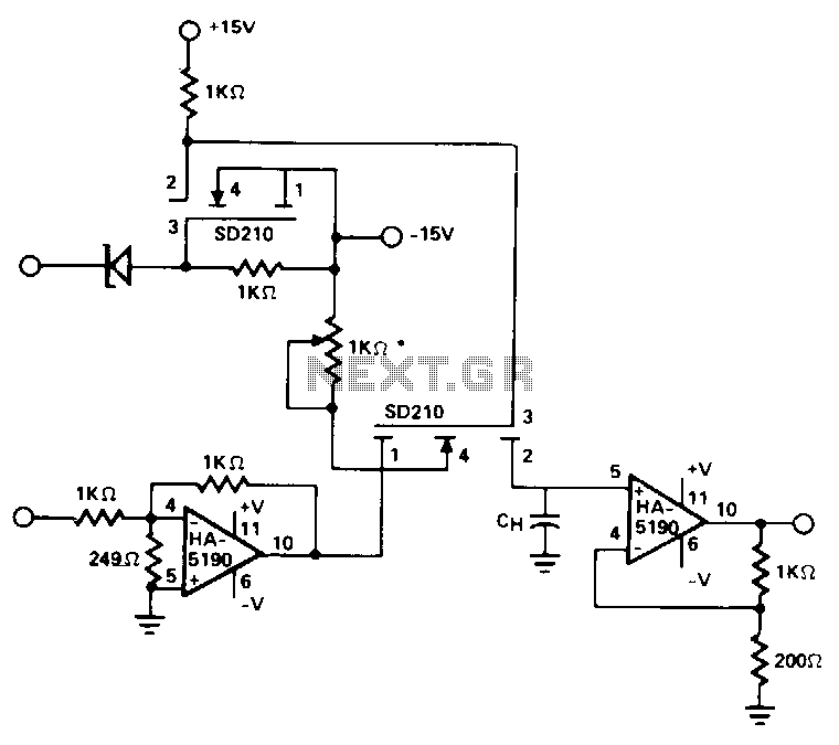
This circuit utilizes the speed and drive capability of the HA-5190 in conjunction with two high-speed DMOS FET switches. The input amplifier is configured to operate at a gain of -5, while the overall circuit gain remains at unity....
More: A comprehensive electronic schematic description is required to provide an overview of the circuit's functionality, components, and operation. The schematic should include a clear representation of the electronic components involved, such as resistors, capacitors, diodes, transistors, integrated circuits,...
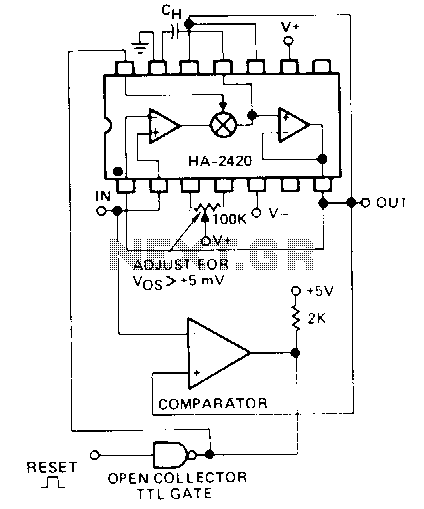
The sample-and-hold function has often been accomplished with separate analog switches and operational amplifiers. These designs typically involve performance trade-offs between acquisition time, charge injection, and droop rate. The HA-242/2425 monolithic sample-and-hold has many improved trade-offs and generally a...
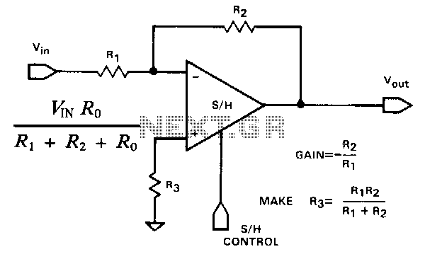
This illustrates another application in which the hookup versatility of a sample-and-hold often eliminates the need for a separate operational amplifier and a sample-and-hold module. This hookup will have a somewhat higher input-to-output feedthrough during hold than the non-inverting...
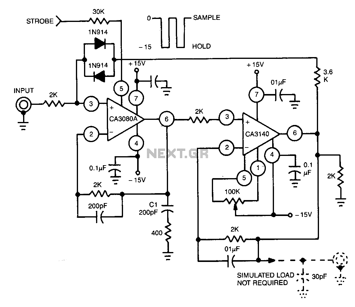
This circuit utilizes a CA3140 BiMOS operational amplifier as the readout amplifier for the storage capacitor C1, while a CA3080A variable operational amplifier serves as the input buffer amplifier and low feedthrough transmission switch. Additionally, offset nulling is achieved...
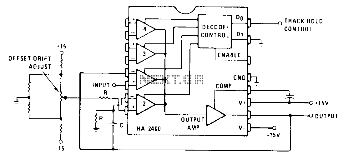
Channel 1 is configured as a voltage follower and is activated during the track/sample time. If the product of R and C is sufficiently short compared to the period of maximum output frequency or sample time, then C will...