
Sample-and-hold

The HA-242/2425 monolithic sample-and-hold circuit is designed to optimize the performance of sample-and-hold applications in various electronic systems. By integrating the sample-and-hold functionality into a single monolithic package, the HA-242/2425 minimizes the complexities associated with discrete component solutions, such as analog switches and operational amplifiers.
The circuit architecture employs a complementary bipolar transistor configuration that enhances the device's ability to handle high charging currents, rated at 30 mA. This high current capability is crucial for applications requiring rapid response times, as it allows for quick charging of the hold capacitor. The feedback mechanism incorporated within the design further ensures that the output voltage remains stable and accurate during the sample-and-hold process.
Charge injection, a critical parameter in sample-and-hold circuits, is minimized to just 10 pC. This low level of charge injection is essential for maintaining signal integrity, particularly in high-precision applications where even minor charge disturbances can lead to significant errors in the sampled signal.
Additionally, the HA-242/2425 features an ultra-low off leakage current of 5 pA. This characteristic is particularly advantageous in applications where the sample-and-hold circuit is not continuously active, as it significantly reduces power consumption and prevents unwanted signal degradation during the hold phase.
The versatility of the HA-242/2425 extends beyond standard sample-and-hold applications. It can also function effectively as an integrator reset switch, allowing for precise control over integration processes in analog signal processing. Furthermore, its low charge injection and leakage characteristics make it an excellent choice for use as a precision peak detector, ensuring that peak values are accurately captured and held for subsequent processing.
In summary, the HA-242/2425 monolithic sample-and-hold circuit offers superior performance, lower costs, and enhanced functionality compared to traditional discrete designs, making it a preferred choice for engineers seeking reliable and efficient solutions in analog signal processing applications.The sample-and-hold function has often been accomplished with separate analog switches and op amps. These designs always involve performance tradeoffs between acquisition time, charge injection, and droop rate.
The HA-242-/2425 monolithic sample-and-hold. has many better tradeoffs, and usually a lower total cost than the other approaches. The switching element is a complementary bipolar circuit with feedback, which allows high charging currents of 30 mA, a low charge injection of 10 pC, and an ultra-low off leakage current of 5 pA; a combination that is not approached in any other electronic switch. These factors make it also superior as an integrator reset switch, or as a precision peak detector.
Related Circuits
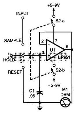
This circuit demonstrates the principle of the sample-and-hold circuit. SI can be replaced by electronic switches (FET, etc.) in an actual application. The sample-and-hold circuit is an essential component in various analog-to-digital conversion applications. Its primary function is to capture...
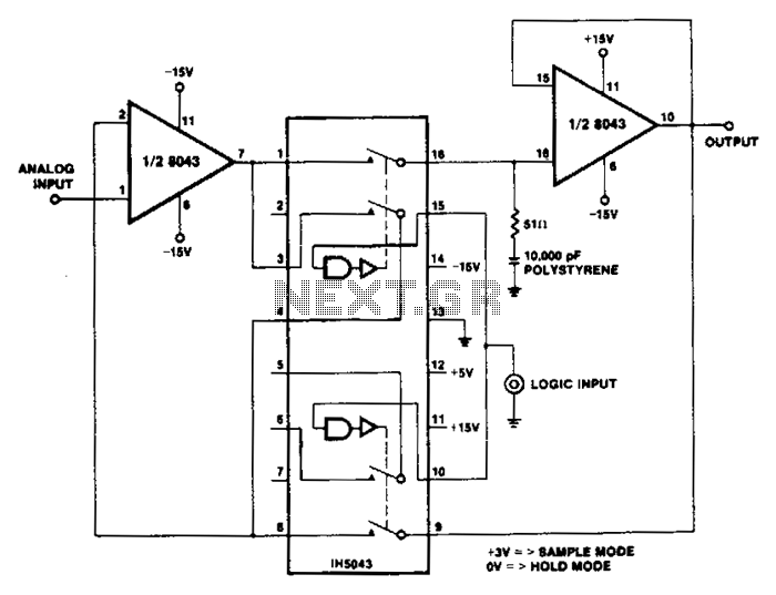
Two significant characteristics of the 8043 are utilized effectively in this circuit. The low input bias currents result in slow output decay rates (droop) during the hold mode, while the high slew rate of 6 V/µs enhances the tracking...
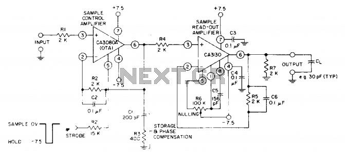
The circuit utilizes a CA3130 BiMOS operational amplifier as the sample-readout amplifier for the storage capacitor C1, while a CA3080A serves as the sample-control amplifier. Applications in linear systems that temporarily store analog data encompass digital voltmeter (DVM) systems,...
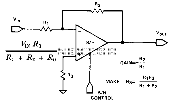
This illustrates another application in which the hookup versatility of a sample-and-hold often eliminates the need for a separate operational amplifier and a sample-and-hold module. This hookup will have a somewhat higher input-to-output feedthrough during hold than the non-inverting...
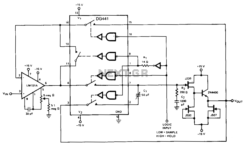
The LM101A provides gain and buffers the input from storage capacitor C2. R2 adds a zero in the open loop response to compensate for the pole caused by the switch resistance and C2, improving the closed-loop stability. R1 provides...
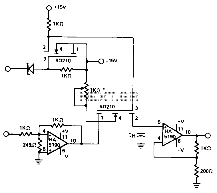
This circuit utilizes the speed and drive capability of the HA-5190 in conjunction with two high-speed DMOS FET switches. The input amplifier is configured to operate at a gain of -5, while the overall circuit gain remains at unity....