
Sample-and-hold

The circuit architecture comprises two main components: the CA3140 BiMOS op amp and the CA3080A variable op amp. The CA3140 is designed to function as a readout amplifier, interfacing with the storage capacitor C1. This configuration allows for effective signal amplification while maintaining high input impedance, which is critical for minimizing loading effects on the capacitor.
The CA3080A, on the other hand, is employed as an input buffer amplifier. This variable op amp is particularly advantageous in applications requiring low feedthrough, as it provides isolation between the input signal and the subsequent stages of the circuit. By utilizing the CA3080A as a transmission switch, the circuit can efficiently manage signal routing without introducing significant distortion or noise.
Offset nulling is an essential feature in precision applications, and the CA3140 facilitates this by allowing adjustments to be made to the output signal. This capability ensures that any inherent offset voltage can be compensated, thereby enhancing the overall accuracy of the readout.
In summary, this circuit design effectively integrates the CA3140 and CA3080A to create a robust system for signal processing, characterized by high fidelity and low distortion. The combination of these components ensures reliable performance in various electronic applications, particularly where precision and signal integrity are paramount.This circuit uses a CA3140 BiMOS op amp as the readout amplifier for the storage capacitor Cl, and a CA3080A variable op amp as input buffer amplifier and low feedthrough transmission switch. Offset nulling is accomplished with the CA3140.
Related Circuits
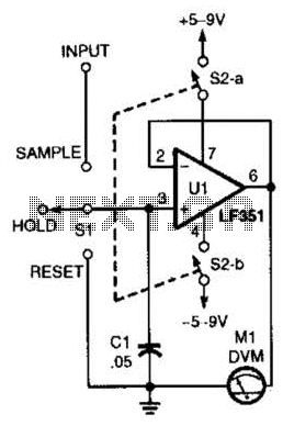
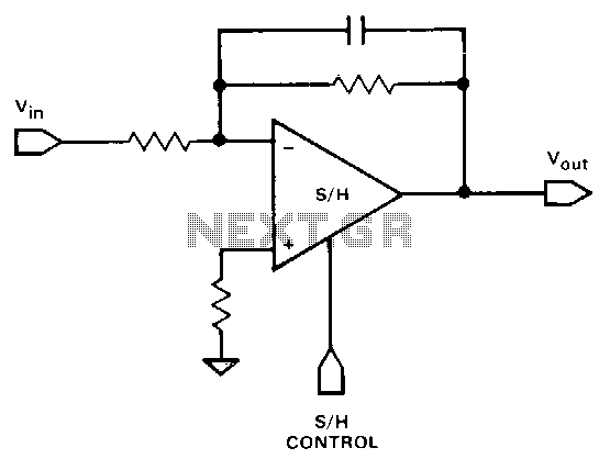
This circuit demonstrates the principle of the sample-and-hold circuit. SI can be replaced by electronic switches (FET, etc.) in an actual application. The sample-and-hold circuit is an essential component in various analog-to-digital conversion applications. Its primary function is to capture...
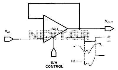
Feedback operates similarly to a conventional operational amplifier (op-amp) voltage follower, providing 11 unity-gain, non-inverting outputs. This configuration also features a very high input impedance. The primary distinction between a track-and-hold and a sample-and-hold lies in the duration for...
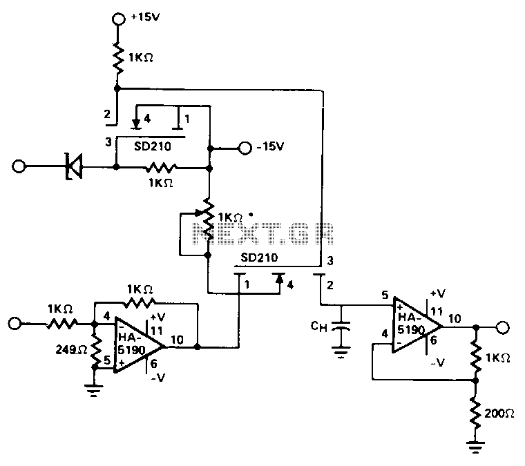
This circuit utilizes the speed and drive capability of the HA-5190 in conjunction with two high-speed DMOS FET switches. The input amplifier is configured to operate at a gain of -5, while the overall circuit gain remains at unity....
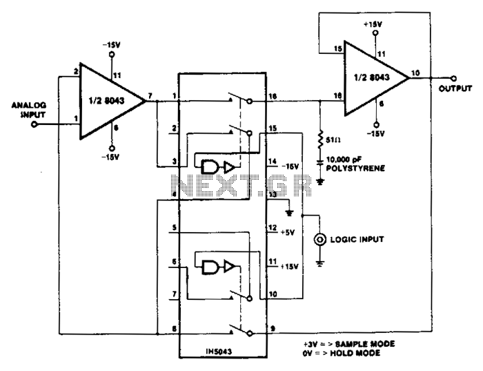
Two significant characteristics of the 8043 are utilized effectively in this circuit. The low input bias currents result in slow output decay rates (droop) during the hold mode, while the high slew rate of 6 V/µs enhances the tracking...
It is often necessary to filter a signal prior to sampling. This can be achieved using a single device. Any of the inverting or non-inverting filters that can be constructed with operational amplifiers (op-amps) may be utilized. However, it...
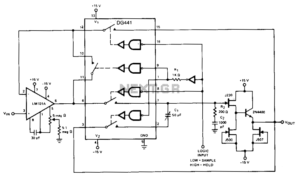
The LM101A provides gain and buffers the input from storage capacitor C2. R2 adds a zero in the open loop response to compensate for the pole caused by the switch resistance and C2, improving the closed-loop stability. R1 provides...