
Sample-and-hold

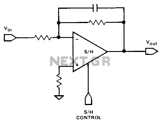
The LM101A operational amplifier is utilized in a sample-and-hold circuit to ensure precise signal processing. The configuration begins with the input signal being buffered by the LM101A, which amplifies the signal while maintaining its integrity. The storage capacitor C2 plays a crucial role in holding the voltage level for processing. The resistor R2 introduces a zero in the open-loop frequency response, which effectively compensates for the pole formed due to the interaction between the switch resistance and C2. This compensation enhances the closed-loop stability of the circuit and ensures reliable performance during operation.
R1 is strategically placed to provide a slight delay in the digital drive signals sent to pins 1 and 9 of the LM101A. This delay can help mitigate issues related to timing mismatches in the circuit, ensuring that signals are properly synchronized during the sample-and-hold process. The capacitor C1 is critical for canceling any coupled charge that might interfere with the accuracy of the sample-and-hold function. By maintaining the sample-and-hold offset below 5 mV across the specified analog signal range of -10 V to +10 V, the circuit ensures high fidelity in signal reproduction.
The aperture time of the circuit is typically 1 picosecond, which indicates the precision timing capability of the system. The switching time of the DG441, which is used in conjunction with this circuit, also plays a significant role in determining the overall performance. The acquisition time, noted to be 25 picoseconds, can be further optimized by integrating a faster slewing operational amplifier, thereby enhancing the responsiveness of the circuit.
The droop rate, which is observed to be less than 5 mV/s at a temperature of 25°C, reflects the stability of the stored voltage over time. This characteristic is essential for applications requiring long-duration signal retention without significant degradation, ensuring that the output remains stable and reliable throughout the operation. Overall, the described circuit configuration is designed to provide high-performance signal processing with minimal offsets and optimal stability.The LM101A provides gain and buffers the input from storage capacitor C2. R2 adds a zero in the open loop response to compensate for the pole caused by the switch resistance and C2, improving the closed-loop stability. R1 provides a slight delay in the digital drive to pins 1 and 9. C1 provides cancellation of coupled charge, keeping the sample-and-hold offset below 5 mV over the analog signal range of -10 through +10 V.
Aperture time is typically 1 p.s, the switcl>.ing time of the DG441. Acquisition time is 25 p.s, but this can be improved by using a faster slewing op amp. Droop rate is typically less than 5 mV/s at 25°C.
Related Circuits
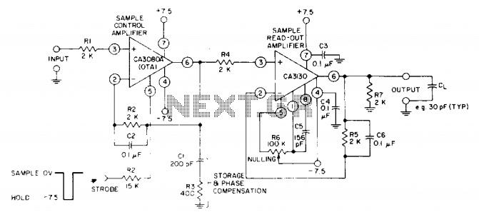
The circuit utilizes a CA3130 BiMOS operational amplifier as the sample-readout amplifier for the storage capacitor C1, while a CA3080A serves as the sample-control amplifier. Applications in linear systems that temporarily store analog data encompass digital voltmeter (DVM) systems,...
It is often necessary to filter a signal prior to sampling. This can be achieved using a single device. Any of the inverting or non-inverting filters that can be constructed with operational amplifiers (op-amps) may be utilized. However, it...
More: A comprehensive electronic schematic description is required to provide an overview of the circuit's functionality, components, and operation. The schematic should include a clear representation of the electronic components involved, such as resistors, capacitors, diodes, transistors, integrated circuits,...
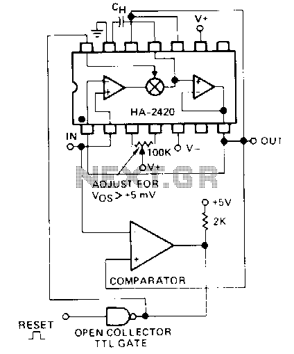
The sample-and-hold function has often been accomplished with separate analog switches and operational amplifiers. These designs typically involve performance trade-offs between acquisition time, charge injection, and droop rate. The HA-242/2425 monolithic sample-and-hold has many improved trade-offs and generally a...
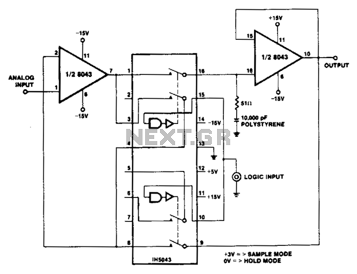
Two significant characteristics of the 8043 are utilized effectively in this circuit. The low input bias currents result in slow output decay rates (droop) during the hold mode, while the high slew rate of 6 V/µs enhances the tracking...
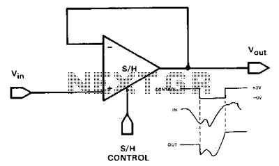
Feedback operates similarly to a conventional operational amplifier (op-amp) voltage follower, providing 11 unity-gain, non-inverting outputs. This configuration also features a very high input impedance. The primary distinction between a track-and-hold and a sample-and-hold lies in the duration for...