
schematic dac0800 introduction

The circuit described involves several critical components and configurations to achieve the desired functionality. The Op-Amp 741 is a versatile operational amplifier that provides gain and isolation, ensuring that the output signal is compatible with the 5V speaker used as an alarming device. The DAC0800, a high-performance digital-to-analog converter, facilitates rapid conversion of digital signals from the microcontroller into analog voltages, which are necessary for driving the speaker.
In addition to the primary components, the circuit employs a low-pass filter to smooth the output of a square wave generated by the microcontroller. The filter's cutoff frequency is strategically set to allow only the average value of the square wave to pass through, effectively transforming it into an analog signal. The variable duty cycle of the square wave is adjusted to control the output voltage, providing flexibility in the alarming signal's amplitude.
The operational setup requires careful measurement and calibration. The reference resistor (Rref) plays a crucial role in determining the output current (IFS), and it should be measured accurately to ensure proper functioning of the circuit. The voltage across Vref is a key parameter that influences the performance of the DAC, and it should be monitored throughout the testing phase to validate the circuit's response to varying input voltages.
By executing the program designed to manipulate the low-pass filter and output compare functions, the circuit can generate a range of analog voltages corresponding to different digital inputs. This capability allows for comprehensive analysis and fine-tuning of the alarming device's response, ensuring that it operates effectively within its specified voltage range.analog voltage get amplified and isolated from the controller circuit hence the Opamp circuit is used to provide the compatibility with the alarming device. In our circuit we have used a speaker as an alarming device which is operable on 5V. We have used the DAC to convert the digital data coming from the micro-controller to an analog alarming dev
ice, this is done by using an opamp 741 at the output of DAC so that the analog voltage get amplified and isolated from the controller circuit hence the Opamp circuit is used to provide the compatibility with the alarming device. In our circuit we have used a speaker as an alarming device which is operable on 5V. The DAC0800 provides high speed digital to analog conversion. When very low conversion rates can be used, another method of digital to analog conversion may suffice.
Consider a square wave which is input to a low pass filter, whose cutoff frequency is far below the repetition rate of the square wave. From Fourier analysis, only the average value of the square wave should pass through the filter. By varying the duty cycle for the square wave, the average value o f the wave can be changed. Therefore, a low pass filter and the output compare functions can be used together to form a simple D/A converter for slowly varying signals.
Write a program that uses the low pass filter in Figure 2 as a D/A converter. Accept a voltage, between 0V and 5. 0V, and use a 10KHz wave with variable duty cycle to produce the proper output voltage. The output compare functions should be used to generate the square wave. Measure Rref with an ohmmeter. Connect the circuit in Figure 1. Measure the voltage dropped across Vref and calculate IFS. Run the program for several voltages and analyze the results. 🔗 External reference
Related Circuits
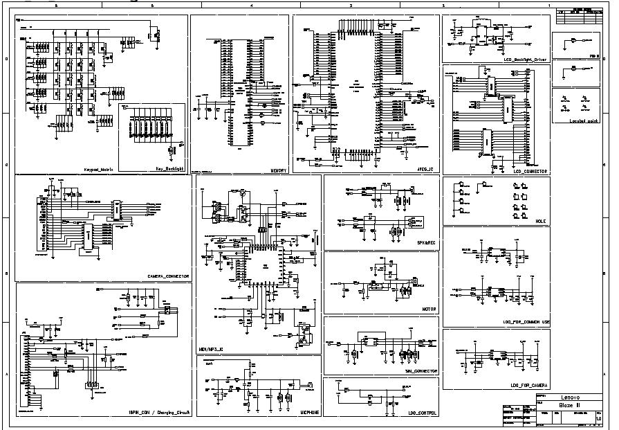
General use camera backlighting baseband circuit: the circuit includes a table of contents, Calyso, iota, matrix, keypad key, memory, IC image, LCD connector, LCD backlight driver, locate points, holes, Speaker4, camera connector, motor, MIDI/MP3 ICs, charging circuit, microphone phone,...
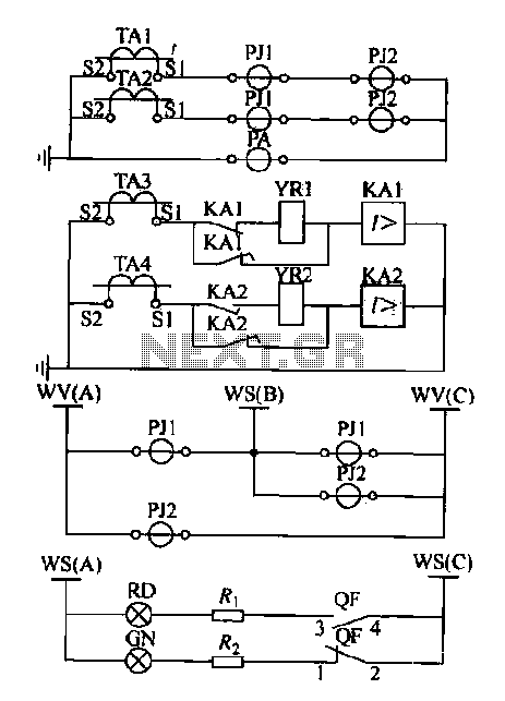
Expanding schematic circuit for the secondary circuit of high-voltage lines. The schematic circuit for the secondary circuit of high-voltage lines is designed to enhance the distribution and management of electrical power in high-voltage systems. This circuit typically includes components...
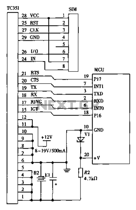
The design of a wireless data communication circuit is primarily intended for motor vehicles and fixed base station systems to facilitate close-range wireless data exchange. The circuit is based on the core chip nRF401 and its associated components. The...
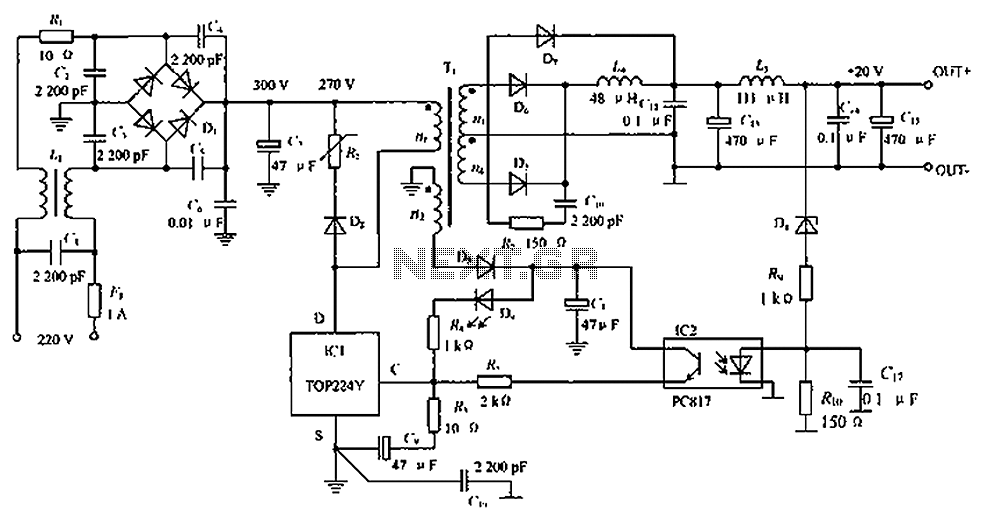
The circuit depicted in the figure is designed to achieve a higher power output by modifying specific components. On the left side of the figure, components R1, L1, D1, and capacitors C1 to C7 form a conventional filtering and...
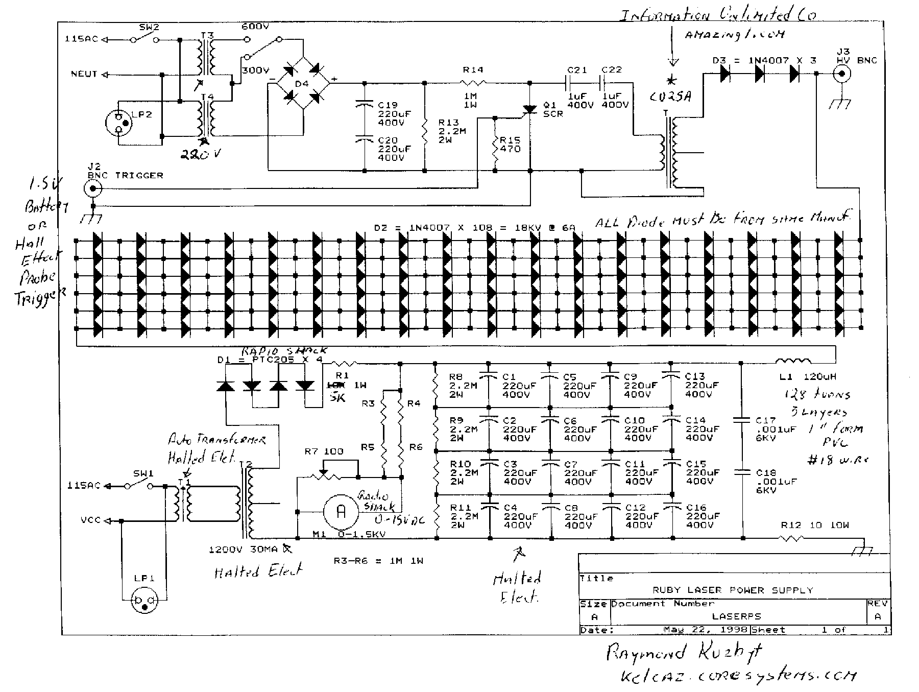
This chapter includes circuit diagrams for various power supplies designed for pulsed solid-state lasers. It features units that are compatible with the widely used Hughes ruby and YAG rangefinder laser assemblies, one utilizing the flash from a disposable pocket...
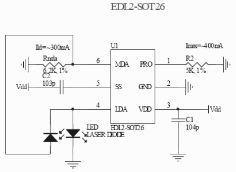
Continuous wave (CW) operation is achievable with a current of up to 350 mA from a supply voltage range of 2 to 6 V. The system supports TTL modulation frequencies of up to 10 kHz, with an adjustable duty...