
schematics Buck switching regulator based on ATtiny84a -- please critique!

The circuit design requires significant improvements in several areas to ensure reliable operation under high-current conditions. To enhance the gate drive, implementing a dedicated gate driver IC that can provide sufficient current to quickly charge and discharge the gate capacitance of the MOSFET is essential. This will minimize switching losses and improve overall efficiency. Transitioning to an N-channel MOSFET will also reduce conduction losses due to its lower Rdson.
Incorporating proper thermal management is crucial, especially considering the high power levels involved. This includes selecting appropriate heat sinks and ensuring adequate airflow around the components.
For the feedback network, using a combination of resistive and capacitive elements will help stabilize the control loop and mitigate the effects of noise and ripple. The addition of an error amplifier with compensation will enhance the performance of the comparator, allowing for better control of the output voltage and improved transient response.
The output filter design should also be revisited to ensure that it can handle the expected ripple current without saturating. Selecting an inductor with a higher current rating and ensuring that the capacitors are rated for the appropriate voltage and ripple current will enhance reliability.
Overall, addressing these design considerations will lead to a more robust and efficient power supply capable of handling high currents safely and effectively.The microcontroller won`t be able to drive the gate of Q1 very hard (usually GPIO pins can only source a few milliamps) so your turn-on and turn-off will be very slow. This will limit how well your high-side switch will behave. You don`t have a gate-to-source resistor on Q1, so you`re solely dependent on the GPIO keeping the MOSFET on or off.
If t he GPIO pin goes high-impedance, the MOSFET may turn itself on if the gate picks up a charge from the environment. which is crazy high power since D is going to be high (input is close to output). Also, the 225mA or so that will flow will also be burned in Q1, which isn`t healthy since it`s a relatively small device.
Your purely resistive feedback network is a bad idea. You really need some compensation and/or filtering. Your comparator will be hyper-fast and could react to switching noise, pickup, ripple, etc. - since you don`t seem to be using an error amplifier with compensation to control the gain and phase, you`re going to need some cap across R5 (and some luck). You don`t have input reverse-polarity protection and an input fuse in your power train. Big no-no, especially when the source is battery-based (big short-circuit sourcing capability). That being said, this isn`t a simple project by any stretch. Your schematic is largely incomplete and lacks basic safety protection that any power supply (especially ones that run at high power levels like yours) will need.
Even after the good answer by Madmanguruman, there are additional things that should be noted. The main difficulty with this design will be the high current being processed. I`ll pay attention mainly to the power processing components, power modulator, and filtering. Power FET is P channel. IRF4905: Rdson=0. 02@25C, 0. 034@150C; Ciss=3500pF. Conduction loss will be very high. For Vin=16. 8V, Vo=12V, Iout=40A, Pcond = $ ext{D } ext{Iout}2 ext{Rds}$ = (. 7)(1600)(0. 034) = 38W. After considering the thermal resistance of the TO220 package and case to sink junction, a heatsink with 2C/W will be required to meet 150C junction with an ambient temp of 25C. It is much better to use N channel FETs for high current situations. An otherwise equivalent N channel FET will have 1/3 the Rdson as a P channel FET. Gate Drive. There is no adequate gate drive in this design. Especially for turn off. With 70 Ohm turning off a FET with Ciss of 3500pF, turn off time will be at least 500nSec. This will mean huge switching loss in the FET, probably at least 15W of additional loss in the FET. This design has to have a much better gate drive. Since the gate drive needs to be improved anyway; it would be very beneficial to change to an N channel switching FET, and use a matching synchronous rectifier with a gate drive IC (like IR2104 or LM5104 or some such).
Hysteretic Control. There is no problem with constant on time, variable off time control. Hysteretic control can (if you are careful) work well, and have excellent transient response. But, the problem here is using the comparator in the uC. There needs to be access to the comparator to provide added hysteresis. So, a comparator with hysteresis, and with a response time less than 500nSec needs to be added. You would want to add hysteresis of about 100mV. Output filter. Good inductor, L1. At 40A plus ripple current it will be on the verge of saturation. It would be better to have a higher current part, but it is not a major concern. It looks like the output capacitors C1 and C2 are ceramic, which is a good choice, should be able to have a total ESR of less than 20 mOhms for a ripple voltage ~100mV. It is interesting, that the load resistance at maximum load (~0. 3 Ohms) is very close to the characteristic impedance of the output filter (~0. 2 Ohms). This is lucky, since it means that the filter is well damped, more about this later. If you are only driving motors with this supply there 🔗 External reference
Related Circuits
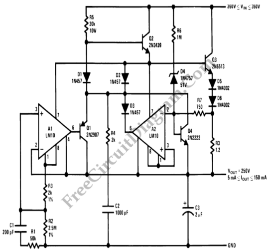
This circuit is a high voltage regulator that features foldback current limiter protection. It utilizes the LM10 comparator along with a voltage reference in its core design. The high voltage regulator circuit is designed to maintain a stable output voltage...
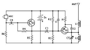
4 Stage FM Transmitter. This FM transmitter circuit utilizes four radio frequency stages, functioning as a VHF oscillator. It is available for wholesale through fmuser, including the CZE and CZH models of FM transmitters, which are suitable for OEM...
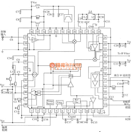
MRFICl505R2 is a 1.575GHz GPS downconverter chip. It integrates a mixer, VCO, PLL, crystal oscillator, A/D converter, loop filter, and other circuits. The MRFICl505R2 IF output frequency is 4.1MHz, with a typical conversion gain of 105dB, an operating voltage...
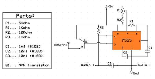
Planning to base a QRP transmitter on an instructables project, utilizing a large collection of 555 integrated circuits available. The issue is that this transmitter is designed to operate slightly below the commercial AM band. The goal is to...
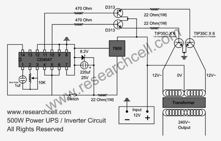
This circuit diagram features a single variable resistor utilized to adjust the frequency of a 240V AC output current. It is advisable to use a frequency meter to modify the frequency from 50Hz to 60Hz according to specific requirements....
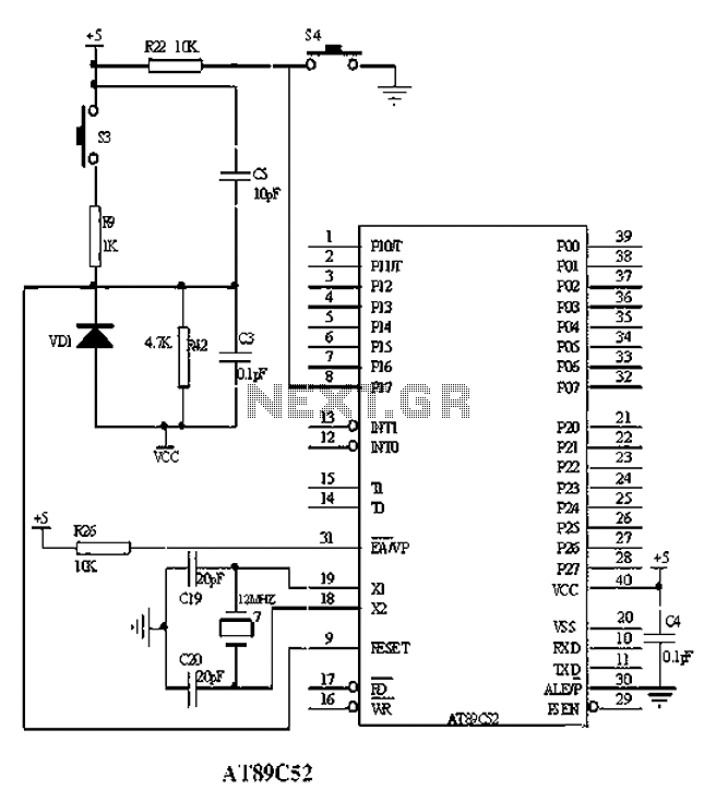
The American Atmel AT89C52 is a low-voltage, high-performance CMOS 8-bit microcontroller chip that contains 8KB of rewritable program memory and 256B of random access data memory (RAM). Atmel's high-density devices utilize non-volatile memory technology and are compatible with the...