
Secret Ethernet optical wireless communication drive circuit diagram
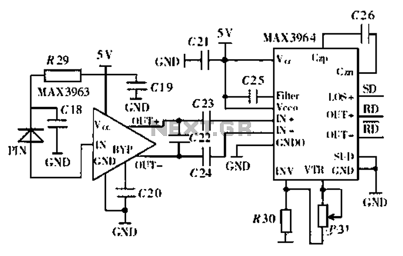
The described circuit utilizes the MAX3263 chip, which integrates a high-speed modulation driver capable of operating at frequencies exceeding 155 MHz. This feature is crucial for applications requiring rapid data transmission, such as Ethernet over laser communication. The modulation driver circuit is designed to accommodate the specific requirements of laser diodes, including the need for precise biasing and monitoring of output power.
The modulation driver employs a feedback mechanism that ensures the stability of the laser's output. By adjusting the resistor values, particularly R28 and R26, the circuit can optimize the laser's performance, balancing the extinction ratio and output power. The careful selection of resistors allows for fine-tuning of the modulation current, which is critical in maintaining signal integrity in high-speed communication systems.
The integration of a monitor diode within the laser diode assembly plays a pivotal role in maintaining consistent output power. As the light intensity fluctuates, the monitor diode generates a feedback current that is used to adjust the bias current, thereby stabilizing the output. This closed-loop control system is essential for preventing signal degradation, particularly in environments where temperature variations may affect diode performance.
The differential PECL signaling used in conjunction with the modulation driver enhances the robustness of the communication link. This signaling method is less susceptible to noise, making it suitable for high-speed data transmission. The circuit design must ensure that the output voltages remain within specified limits to prevent saturation of the laser, which can lead to signal distortion.
In summary, the modulation driving circuit design utilizing the MAX3263 chip is a sophisticated solution for high-speed laser-based Ethernet communication. The combination of precise biasing, feedback control, and differential signaling contributes to a reliable and efficient communication system capable of operating in various environments.Ethernet is the most widely used networking technology with high reliability, media informative, easy to expand and update, etc., in businesses, schools and other fields are wi dely used. According to the standard IEEE802.3 Ethernet specification, each Ethernet coaxial cable length should not exceed 500m, through the repeater interconnection network shall not exceed the maximum distance 2.8km. In this case, the wireless communications using laser technology, beyond the geographical limits of Ethernet data communication needs, has a strong practical value.
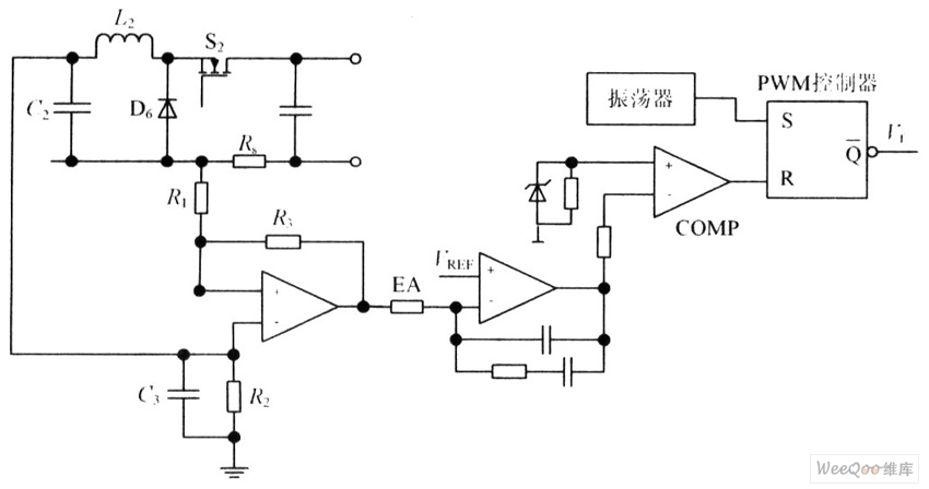
Modulation driving circuit design 6 is a circuit diagram of a modulation drive, mainly by MAXIMs MAX3263 chip and internal 155MHz with monitor diode laser LD constitution. MAX3263 main internal bias supply provides temperature compensated bias and reference voltage output Vref1 and Vref2, through a resistor R25, R26, R27 and R28 of the internal high-speed modulation driver circuit, laser diode and monitoring program.
MAX3263 output current are inside the mirror current source control, the current mirror has 2Vbe junction temperature drift, the reference voltage is set at 2Vbe, junction temperature drift can be canceled. Select resistor R28 to adjust the laser bias current quiescent Ibo, Ibo make slightly less than the laser threshold current, so that the output of the laser has a good extinction ratio.
LD internal monitor diode can light intensity change is converted to a current Ipin, the feedback current generated by the internal conversion Ibs, by the formula Ibo 40 (Ib + Ibs), light intensity change is converted into a portion of the laser bias current, feedback on laser, to ensure stable output optical power. Differential PECL signal RD input from the internal high-speed input buffer and output common-emitter differential-component modulator modulates the size of the modulation current is determined by the R26 current Im decision.
Select R26 size, make appropriate laser modulation current, sufficient output optical power, and has a good extinction ratio. At the same time should be OUT +, OUT- terminal voltage at 2.2V or more to prevent the laser saturation.
Because of Figures 6 and 7 are in the main chip 155MHz or more, so by the two circuit transceiver circuit, careful parameter selection and PCB design can be applied to high-speed optical communications applications. 5 system test on the basis of various parts of the design, the linking them, in the absence of optical antenna conditions, successfully conducted experiments indoor laser wireless Ethernet communication.
Improve the system now, and ready to be used in optical networks.
Related Circuits
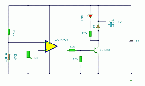
A thermistor positioned as indicated creates a heat-activated sensor. Variations in temperature will modify the output of the operational amplifier, triggering the relay and illuminating the LED. Reversing the placement of the thermistor and the 47k resistor converts the...
This electronic pressure gauge utilizes a Wheatstone bridge-type pressure sensor to drive a 3 A digit A/D converter and a display. IC1 is a quad op-amp that interfaces the bridge sensor to the A/D converter. R16 allows for zero...
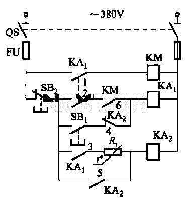
Competition among relay contacts in contactor control systems often leads to significant issues that can be cumbersome to address. In some cases, this requires the addition of numerous components. However, utilizing a negative temperature coefficient thermistor (NTC) for delay...
The circuit is capable of enhancing the system power factor to a value exceeding 0.99. It effectively reduces the waveform distortion of the input supply current, ensuring compliance with GB15144 standards, with a distortion index lower than level L....
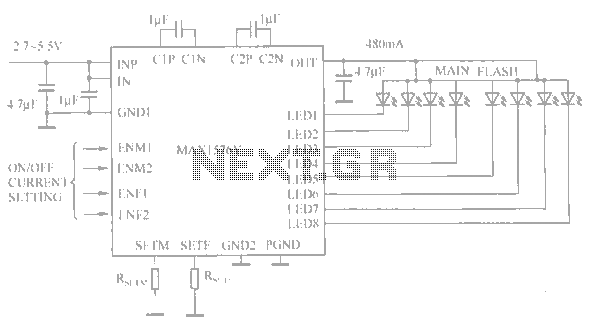
The circuit utilizes the MAX1576Y charge pump white LED driver, capable of supplying a total current of up to 480mA across two groups (n = 4 white LEDs). Each white LED in the flashing group can draw a maximum...
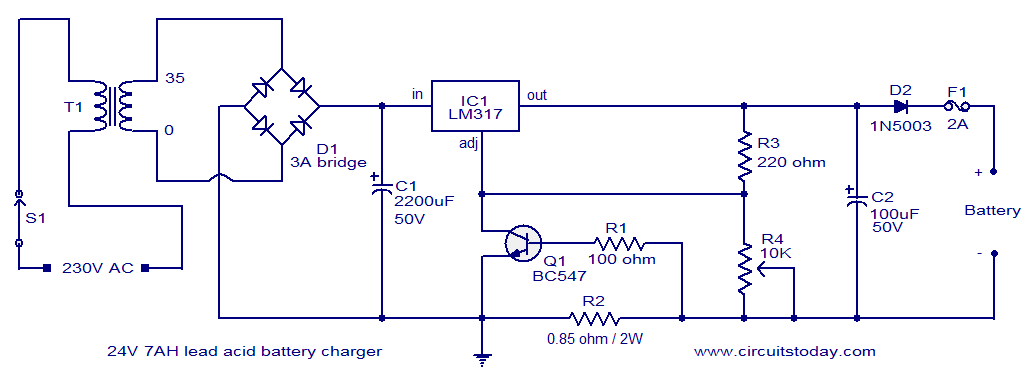
This lead-acid battery charger circuit is designed based on a request from Mr. Devdas C. His requirement was for a circuit that could charge two 12V/7AH lead-acid batteries connected in series. He did not specify the number of cells...