
Self Retriggering Timed Generator Circuit
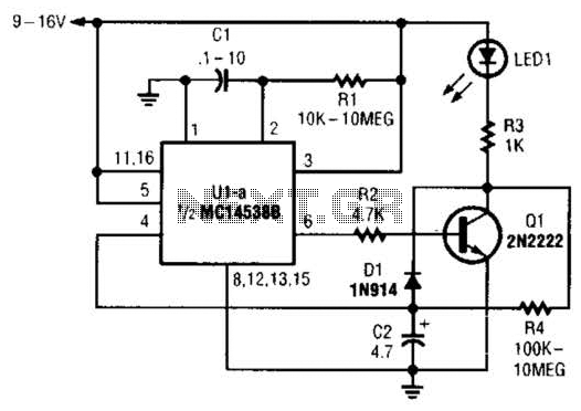
The circuit operates as a timing mechanism, utilizing a feedback loop involving charging and discharging of capacitor C2 to create a repeating cycle. The charging phase occurs when the circuit is powered, leading to a gradual increase in voltage across C2. This voltage is monitored by operational amplifier U1, which serves as a comparator. Once the voltage exceeds the threshold defined by U1, it triggers a high output state at pin 6. This output activates transistor Q1, allowing for rapid discharge of C2 through D1, effectively resetting the cycle.
The resistors R3 and R4 are crucial in determining the charging rate of C2. Their values influence the time constant of the RC circuit formed, which in turn affects the frequency of the oscillation. The capacitor C2's value also plays a significant role in the timing; larger capacitance will result in longer charge times, while smaller capacitance will shorten the cycle. Fine-tuning R4 allows for precise adjustments to achieve the desired timing characteristics, accommodating variations that may arise due to component tolerances or supply voltage changes.
Diode D1 is included to ensure that the discharge path for C2 is unidirectional, preventing any potential feedback that could disrupt the intended operation of the circuit. The visual indicator LED1 provides feedback to the user, illuminating during the charging phase and turning off when the circuit transitions to the discharge phase.
In summary, this circuit exemplifies a simple yet effective timing mechanism, with parameters that can be adjusted to tailor the performance to specific requirements. The interplay between the components creates a reliable oscillation, suitable for applications such as blinking lights, timers, or other periodic signal generation tasks. When power is first applied to the circuit, 02 begins to charge via LED1, R3, and R4. When the voltage across C2 reaches Ul`s input trigger level, the output of Ul at pin 6 goes positive for a period that is determined by the values of and it! r That turns Ql on, discharging 02 through D1 and Ql. At the end of the set period, the output of Ul at pin 6 goes low, turning Ql off and allowing the current to begin flowing through LED1, R3, and R4 to gain charge 02, causing the cycle to repeat.
The repeat time is determined by the values of R3, R4, and C2. The previous formula won`t be as accurate for this circuit, but it will at least get you close enough for the capacitor value; then R4 can be fine-tuned to obtain the desired timing period. 🔗 External reference
Related Circuits
The siren circuit plays a crucial role in various alarm systems, including emergency alerts, burglar alarms, fire alarm circuits, timers, and sensor controls. Without these circuits, it would be impossible to recognize the intended functionality. The operation of the...
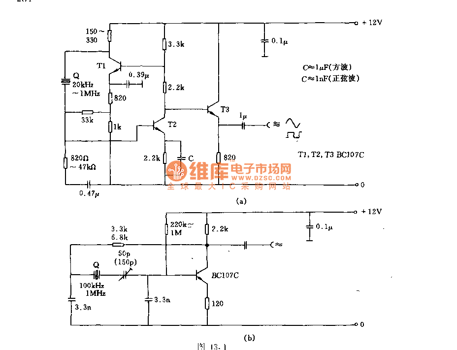
Figures (a) and (b) illustrate two basic oscillator circuits operating at 2 MHz. The circuit design allows for adjustment of the optimal operating point through testing. The two oscillator circuits depicted in the figures utilize different configurations to achieve stable...
The wire connected to the 5V pin is linked to the positive pins of the breadboard, which are not connected to any other components. There are no additional connections on the positive column. While this may seem like a...

The motorcycle anti-theft alarm circuit consists of several components, including the anti-theft detection circuit, the control circuit, the sound generator, the audio oscillator, and the power amplifier output circuit, as illustrated in figure 7-91. The anti-theft detection circuit is...
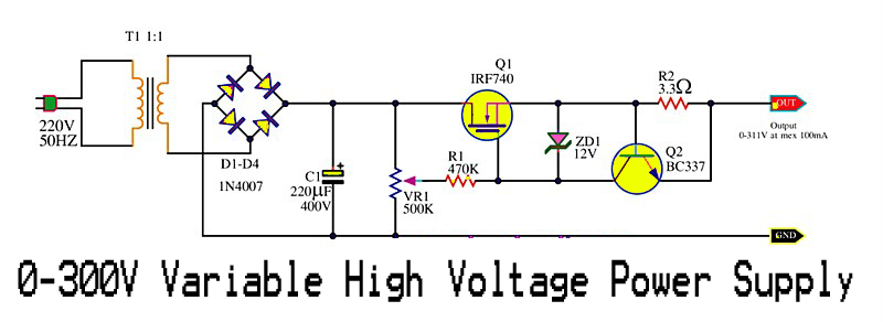
This is a variable high voltage DC power supply circuit that allows for customization of the output voltage ranging from 0 to 311V DC. It includes a current limit protection feature set at approximately 100 mA. The power MOSFET...
The transistors create a differential pair with an active current-source tail. This configuration, referred to as a variable-transconductance multiplier, produces an output that is proportional to the product of the two input signals. The multiplication effect arises from the...