
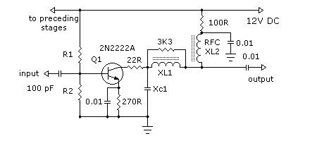
Signal Amplifier with 2N2222
If the emitter voltage is 2.35V approx. then the emitter current Ie through the emitter resistor of 270 ohms must be (from ohms law) 2.35 / 270 = 0.0087 or 8.7 mA. I've also said elsewhere I like base current to be about 1/7th of emitter current - alright these are my foibles and others would disagree. They're welcome to write their own papers.
So base current is going to be about 1 mA and seeing R1 + R2 are connected across 12V it follows that (from ohms law) R1 + R2 = 12V / .001 = 12,000 ohms or 12K. For biasing R1 is 3 times R2 so using simple maths R2 is 25% or 3K and R1 would be 9K which are not necessarily readily available standard values. We will make R2 = 3K3 and R1 = 10K which if you do all your sums is near enough and probably about a third of the values others might use.
So we have our DC conditions satisfied and the 0.01 capacitor in parallel with the emitter resistor means for RF purposes the emitter is at ground potential. This then leaves the output circuit to be discussed. The 22 ohms resistor in the collector circuit is there to discourage parasitic oscillations. RFC XL2 as I said before is only to decouple the power supply and I'd look for a reactance of around 20,000 ohms or at 2 MHz something like 1 to 2.5 mH.
All this leaves is our low pass filter matching network. First question?? How much output power do we want? Huh? Yep that's how it all works.
Let's say we wanted +17 dBm for a mixer circuit. To the uninformed +17 dBm is a power relationship in milli-watts. Power is always (10 * log of power) so in this case in reverse we divide the 17 by 10 to get 1.7 which is the log of 50 so it follows that +17 dBm is in fact 50 mW of power. Learnt something?
Incidentally a power level of 50 mW into 50 ohms also equates to Erms = SQRT ( 0.05 * 50 ) or 1.58V RMS or 2.828 times that value to get pk-to-pk, which is 4.47V PK-PK.
Alright how do we design to get 50 mW out of our amplifier? By using the formula R = Vcc2 / (2 * Po) or in our case [ (12V * 12V) / (2 * 0.05) ] = 1440 ohms. Want more power? Change the numbers! Obviously there are limits but you get the idea.
From the above the collector needs to see a load of about 1440 ohms which in turn has to be transformed into our 50 ohm load. By the way, if the amplifier doesn't see a 50 ohm load then all these calculations go right out the window. At the end I show my method of ensuring something like a 50 ohm load and more important the method helps the succeeding stage see a 50 ohm source.
If you have done previous tutorials on filters this is easy. If not then you need to do more work. This is a simple "L" network low pass filter designed in this case to transform 1440 ohms to 50 ohms. Follow these steps where SQRT signifies square-root-of:
1. XL = the SQRT of [(R1 * R2) - (R1 * R1)] = SQRT [(50 * 1440) - (50 * 50)] = SQRT [ 72,000 - 2,500] = SQRT of 69500 = 263.6 ohms
2. Xc = [(R1 * R2) / XL] = 72,000 / 263.6 = 273 ohms
Therefore the reactance of our inductor is about 264 ohms at our frequency of interest and the reactance of our capacitor is about 273 ohms at that same frequency. In the beginning I mentioned a requirement for a 1.8 to 2 MHz small signal amplifier so we will nominally use 2 MHz as our cut off frequency i.e. we want to pass all signals below about 2 MHz but not above (filter out harmonics!).
Here I always see what capacitor has a reactance of 273 ohms at 2 MHz using the standard capacitive reactance formula Xc = 1 / (2 * pi * Fo * C). Which when algebraically rearranged for our purposes becomes C = 1 / (2 * pi * Fo * Xc ). Slipping 273 ohms for Xc into that formula and 2 MHz (2,000,000) should get you on your calculator 2.91.. -10 which should then be multiplied by exp 12 to arrive at an answer in pF. Doing that we get an answer of 291 pF which doesn't exist in the real world.
Now you have several choices here. (a) just plonk nearest standard components in for XL and Xc and don't worry about tuning - not recommended. (b) make part of Xc variable e.g. Xc comprises a fixed 270 pF capacitor with a 5 - 50 pF trimmer in parallel or (c) make Xc fixed and XL variable. You can only use the latter option if you have suitable slug tuned inductors available (they ain't cheap but could possibly be salvaged if you know what you are doing).
In the event you chose option (b) the required fixed inductor would be determined from the inductive reactance formula XL = (2 * pi * Fo * L). In ALL examples I use 6.2832 for 2 * pi. For our example we can again rearrange the formula as L = XL / (2 * pi * Fo) and plugging in this case 263.6 ohms XL from above and 2 for 2 MHz we get L = 263.6 / (6.2832 * 2) = 20.98 uH. That is the inductance you would use, possibly with 60 turns of #26 wire on a T68-2 toroid as only one example.
The small signal amplifier described operates within the frequency range of 1.8 to 2.0 MHz, making it suitable for applications in the 160M band. The amplifier circuit is designed to follow a buffer amplifier and is characterized by a class "A" configuration. The key components include a transistor (Q1), biasing resistors (R1 and R2), an emitter resistor (270 ohms), and a low pass filter network for impedance matching.
The biasing network is established to set the base voltage of Q1 to approximately 3V, which is 25% of the supply voltage (Vcc = 12V). The values of R1 and R2 are calculated to maintain this bias point, with R1 set to 10K ohms and R2 to 3.3K ohms, ensuring proper DC operating conditions. The emitter capacitor (0.01 uF) is included to provide RF grounding, stabilizing the amplifier's performance at higher frequencies.
The output stage incorporates a low pass filter designed to match the load impedance of the amplifier to 50 ohms, which is essential for maximizing power transfer. The filter is an "L" network that transforms the higher impedance seen by the collector (approximately 1440 ohms) down to the desired 50 ohm output. This is achieved through careful selection of inductor and capacitor values based on their reactance at the operating frequency.
The design calculations indicate that an inductor with a reactance of approximately 264 ohms and a capacitor with a reactance of about 273 ohms are needed at 2 MHz. A fixed inductor of 20.98 uH can be constructed using a toroidal core, while the capacitor can be implemented with a fixed value in parallel with a variable trimmer capacitor to allow for fine-tuning of the output characteristics.
Overall, this small signal amplifier is structured to provide stable amplification and buffering of RF signals, ensuring compatibility with subsequent stages in a communication system while maintaining the necessary output power levels.A small signal amplifier, perhaps of the type to follow the previous buffer amplifier. We will assume we are buffering and amplifying our signal from the voltage controlled oscillator tutorial. In those examples we were generating and buffering 1.8 to 2.0 Mhz signals for the 160M band. The configuration is much the same as other class "A" amplifier designs covered in previous tutorials.
The output circuit consists of a low pass filter network which also converts the desired output impedance we want Q1 to see to our standard 50 ohms output. The 100 ohm resistor, RFC XL2 and the 0.01 uF capacitors are purely for decoupling purposes i.e., to keep RF out of the small signal amplifier power supply as well as other stages.
Let's consider firstly the input circuit of our small signal amplifier. Q1 is biased for DC conditions by R1, R2 and the emitter resistor of 270 ohms in this instance. Alert readers will be aware I like to bias the base voltage of my transistors to about 25% of Vcc (.25 * 12V) or 3V. It follows then that R1 will be about 3 times the value of R2 - think about it!. If the base voltage is around 3V then the emitter voltage is going to be 3v - 0.65V = 2.35V. Don't follow that? Go back to class "A" amplifier designs covered in previous tutorials. If the emitter voltage is 2.35V approx. then the emitter current Ie through the emitter resistor of 270 ohms must be (from ohms law) 2.35 / 270 = 0.0087 or 8.7 mA.
I've also said elsewhere I like base current to be about 1/7th of emitter current - alright these are my foibles and others would disagree. They're welcome to write their own papers. So base current is going to be about 1 mA and seeing R1 + R2 are connected across 12V it follows that (from ohms law) R1 + R2 = 12V / .001 = 12,000 ohms or 12K.
For biasing R1 is 3 times R2 so using simple maths R2 is 25% or 3K and R1 would be 9K which are not necessarily readily available standard values. We will make R2 = 3K3 and R1 = 10K which if you do all your sums is near enough and probably about a third of the values others might use.
So we have our DC conditions satisfied and the 0.01 capacitor in parallel with the emitter resistor means for RF purposes the emitter is at ground potential. This then leaves the output circuit to be discussed. The 22 ohms resistor in the collector circuit is there to discourage parasitic oscillations. RFC XL2 as I said before is only to decouple the power supply and I'd look for a reactance of around 20,000 ohms or at 2 Mhz something like 1 to 2.5 mH.
All this leaves is our low pass filter matching network. First question?? How much output power do we want? Huh? Yep that's how it all works. Let's say we wanted +17 dBm for a mixer circuit. To the uninformed +17 dBm is a power relationship in milli-watts. Power is always (10 * log of power) so in this case in reverse we divide the 17 by 10 to get 1.7 which is the log of 50 so it follows that +17 dBm is in fact 50 mW of power. Learnt something? Incidentally a power level of 50 mW into 50 ohms also equates to Erms = SQRT ( 0.05 * 50 ) or 1.58V RMS or 2.828 times that value to get pk-to-pk, which is 4.47V PK-PK.
Alright how do we design to get 50 mW out of our amplifier? By using the formula R = Vcc2 / (2 * Po) or in our case [ (12V * 12V) / (2 * 0.05) ] = 1440 ohms. Want more power? Change the numbers! Obviously there are limits but you get the idea. From the above the collector needs to see a load of about 1440 ohms which in turn has to be transformed into our 50 ohm load. By the way, if the amplifier doesn't see a 50 ohm load then all these calculations go right out the window.
At the end I show my method of ensuring something like a 50 ohm load and more important the method helps the succeeding stage see a 50 ohm source. If you have done previous tutorials on filters this is easy. If not then you need to do more work. This is a simple "L" network low pass filter designed in this case to transform 1440 ohms to 50 ohms.
Follow these steps where SQRT signifies square-root-of: 1. XL = the SQRT of [(R1 * R2) - (R1 * R1)] = SQRT [(50 * 1440) - (50 * 50)] = SQRT [ 72,000 - 2,500] = SQRT of 69500 = 263.6 ohms 2. Xc = [(R1 * R2) / XL] = 72,000 / 263.6 = 273 ohms Therefore the reactance of our inductor is about 264 ohms at our frequency of interest and the reactance of our capacitor is about 273 ohms at that same frequency.
In the beginning I mentioned a requirement for a 1.8 to 2 Mhz small signal amplifier so we will nominally use 2 Mhz as our cut off frequency i.e. we want to pass all signals below about 2 Mhz but not above (filter out harmonics!). Here I always see what capacitor has a reactance of 273 ohms at 2 Mhz using the standard capacitive reactance formula Xc = 1 / (2 * pi * Fo * C).
Which when algebraically rearranged for our purposes becomes C = 1 / (2 * pi * Fo * Xc ). Slipping 273 ohms for Xc into that formula and 2 Mhz (2,000,000) should get you on your calculator 2.91.. -10 which should then be multiplied by exp 12 to arrive at an answer in pF. Doing that we get an answer of 291 pF which doesn't exist in the real world. Now you have several choices here. (a) just plonk nearest standard components in for XL and Xc and don't worry about tuning - not recommended.
(b) make part of Xc variable e.g. Xc comprises a fixed 270 pF capacitor with a 5 - 50 pF trimmer in parallel or (c) make Xc fixed and XL variable. You can only use the latter option if you have suitable slug tuned inductors available (they ain't cheap but could possibly be salvaged if you know what you are doing).
In the event you chose option (b) the required fixed inductor would be determined from the inductive reactance formula XL = (2 * pi * Fo * L). In ALL examples I use 6.2832 for 2 * pi. For our example we can again rearrange the formula as L = XL / (2 * pi * Fo) and plugging in this case 263.6 ohms XL from above and 2 for 2 Mhz we get L = 263.6 / (6.2832 * 2) = 20.98 uH.
That is the inductance you would use, possibly with 60 turns of #26 wire on a T68-2 toroid as only one example. 🔗 External reference
Related Circuits
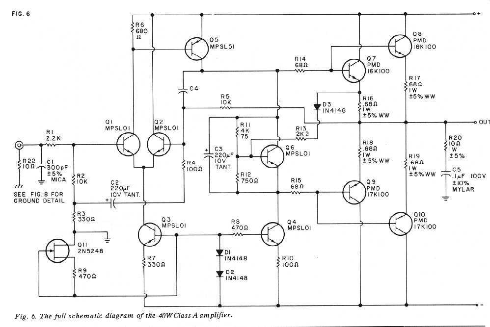
This is a very simple, low-cost, Hi-Fi quality power amplifier. It can be built in five different configurations, as shown in the table, ranging from 20 W to 80 W RMS. The Hi-Fi quality power amplifier circuit is designed to...
By adding only a few components, a temperature- and beta-compensated current sink can be converted into a common-emitter (CE) amplifier that maintains a stable biased operating point. This design concept will demonstrate the process. To implement this design, the primary...
This amplifier circuit is designed to enhance TV signals in the UHF range. It employs a low-noise transistor, providing an amplification of 10 to 15 dB within the frequency spectrum of 400 MHz to 850 MHz. It is crucial...
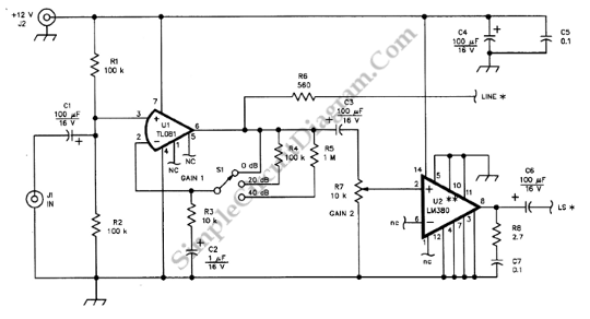
This is a schematic diagram of a general-purpose audio frequency (AF) amplifier circuit. The circuit employs inexpensive 1/4-W resistors, as high precision is not required. The general-purpose audio frequency (AF) amplifier circuit is designed to amplify audio signals for various...
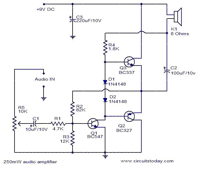
This is a simple three-transistor audio amplifier circuit capable of delivering 250 mW to an 8-ohm speaker. Complementary transistors BC337 and BC227 (Q3 and Q2) are utilized as the output pair, while transistor Q1 (BC547) functions as the preamplifier....
Both parts of the circuit are biased with the constant current sources as shown, and the signal from the collector of the PNP is followed by the Darlington class A output stage whose idle current is controlled by the...