
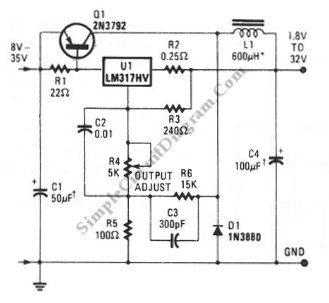
Simple buck mode switching regulator circuit diagram
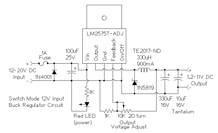
The buck mode switching regulator is a type of DC-DC converter that efficiently steps down a higher DC voltage to a lower DC voltage. The operation of this circuit relies on the principle of pulse-width modulation (PWM), which allows for the adjustment of the output voltage by varying the duty cycle of the switching signal.
In a typical configuration, the circuit consists of a switching element, such as a MOSFET, an inductor, a diode, and a capacitor. The switching element is controlled by a PWM controller, which turns the MOSFET on and off at a high frequency. When the MOSFET is turned on, current flows through the inductor, storing energy in its magnetic field. As the MOSFET turns off, the inductor releases the stored energy, causing the current to flow through the diode and charge the output capacitor.
The output voltage can be regulated by adjusting the duty cycle of the PWM signal. A higher duty cycle results in a longer "on" time for the MOSFET, allowing more energy to be transferred to the output, while a lower duty cycle reduces the output voltage by shortening the "on" time. Feedback mechanisms are often employed to monitor the output voltage and adjust the PWM signal accordingly, ensuring that the output remains stable under varying load conditions.
Overall, the buck mode switching regulator is widely used in applications requiring efficient voltage conversion, such as power supplies for microcontrollers, battery management systems, and various electronic devices. Its high efficiency and compact design make it a preferred choice in modern electronic circuit design.This is a simple buck mode switching regulator circuit diagram. This circuit is more efficient, switch mode regulators convert DC input voltage to pulses of high DC voltage. The DC pulses are used to charge a storage capacitor to the desired output voltage. The voltage is regulated by varying the width of the DC pulse 🔗 External reference
Related Circuits
The objective is to enhance information transmission by utilizing articles. Please contact us via email at [email protected] within 15 days if there are issues related to article content, copyright, or other concerns. Prompt action will be taken to resolve...
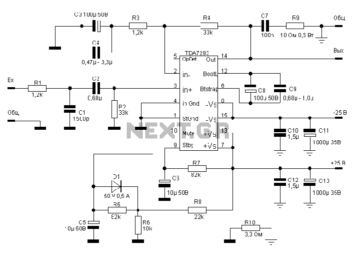
The TDA7293, produced by the ST (SGS-THOMSON) company, is a high-power, high-voltage DMOS high-fidelity amplifier integrated circuit (IC) with a rated output power of 100W. It operates at a maximum voltage of 120V. The key specifications include a dual...
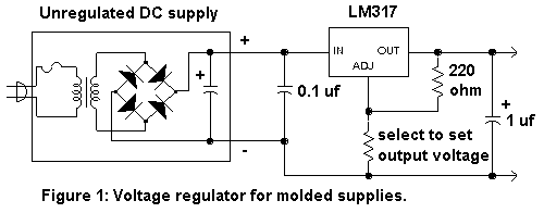
There are a number of ways to obtain the low voltages required to run small projects from the wall power outlet. The simplest way is to buy a factory-built molded supply which is designed to plug directly into the...
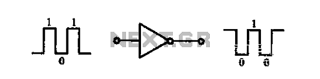
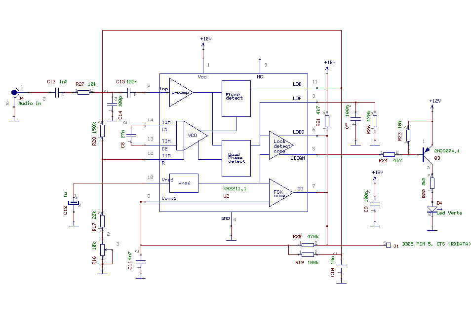
A common-emitter transistor amplifier produces an output signal that is 180 degrees out of phase with the input signal, commonly referred to as an inverting amplifier. When the electrical path for amplifying the pulse signal is activated, this circuit...
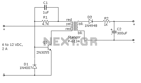
A switching voltage regulator circuit depicted in the schematic diagram can serve as a cost-effective solution for high-efficiency electronic circuit requirements. The switching voltage regulator circuit operates by converting a higher input voltage to a lower output voltage with minimal...
This is an example of a simple inverter that can be used to power a fluorescent lamp and a small strobe. This circuit will produce over 400 VDC from a 12 VDC, 2.5 A. The described inverter circuit is designed...